

Design of magnetron co-sputtering configuration for preparing magnesium tin silicide-based thermoelectric alloy thin films
- Laboratory of Advanced Materials - University of Science, VNU-HCM
- Center for Innovative Materials and Architectures (INOMAR), VNU-HCM
Abstract
Introduction: Magnesium tin silicide (MgSiSn) is known as a good-thermoelectric-performance, safe and cost-efficient alloy material. The goal of this work is to design a magnetron co-sputtering configuration for depositing alloy thin films from three independent metal targets including magnesium (Mg), silicon (Si) and tin (Sn).
Methods: By this solution, the elemental composition of the MgSiSn thin films can be effectively controlled through changing sputtering power of the individual magnetron. The actual values of elemental composition in the as-deposited films were verified by using energy-dispersive X-ray spectroscopy. The as-deposited thin films were investigated carefully by using the X-ray diffraction to recognize crystalline structure characteristics. Most importantly, typically thermoelectric parameters including Seebeck coefficient, electrical conductivity and power factor were indicated as functions of temperature.
Results: The XRD analysis exhibits cubic anti-fluorite-type structure characteristic of the MgSiSn films; however, the presence of segregated Mg phase is still observed. The testing results for the representative MgSiSn thin film with good adherence show the power factor of PF ~15×10-3 W/mK2, as a result of Seebeck coefficient of S ~132 µV/K and electrical conductivity of σ ~9000 S/cm, at 373 K. At higher temperature than 473 K, the semiconducting behavior of the films tends to transform from p-type to n-type.
Conclusion: The three-target co-sputtering configuration shows the possibility of successfully preparing alloy MgSiSn thin films with good adherence on Si substrate. Furthermore, the testing result suggests that the as-deposited MgSiSn thin films have some potential thermoelectric characteristics, which can be improved more significantly.
INTRODUCTION
Magnesium tin silicide (MgSiSn) ternary alloy is one of the best lead-free thermoelectric materials in the medium temperature range (200 – 600C). It has attracted much interest due to constituted composition from the rich-abundant and non-toxic elements2, 1. According to the estimation expression of thermoelectric figure of merit (Z), ZT = Sσ/κ (where S is Seebeck coefficient, σ and κ are electrical and thermal conductivities, respectively), the increase of S, σ values and the reduction of κ value result in enhancement of ZT value. In the case of the MgSiSn alloy, Si replacement of Sn ion not only increases S value owing to the increasing density of state (DOS) in energy-band structure, but also reduces κ value because Sn atom has much heavier mass than Si atom4, 3.
Another method to achieve high ZT value is producing low-dimensional materials due to the quantum confinement, high σ, and low κ values5. Thin film is known as one of the low-dimensional materials, which doping effect and stoichiometry can be controlled. In literature, there have been limited works on the MgSiSn thin films, as compared to the bulk form. Typically, a study on the very thin MgSiSn film (50 – 90 nm) deposited on Si substrate was reported for optoelectronic and thermoelectric applications6. The used deposition technique, however, was a solid phase epitaxy (SPE), which is quite a complicated, expensive and hard-to-control method. Recently, the Al- and Sn-doped MgSi thin films deposited by using low-cost and high-efficiency sputtering method were attracted7. The MgSiSn film was co-sputtered from MgSi and Sn targets. It facilitated to adjust the Sn content. However, the Mg and Si contents were not independent because their vapor pressure is very different.
To solve the above problems, in this work, a new co-sputtering configuration was set up. The magnetron sputtering system was used to prepare the MgSiSn thin films from three independent metal (Mg, Si and Sn) targets. Some electrical and thermoelectric characteristics of the as-deposited MgSiSn thin films were basically investigated.
MATERIALS - METHODS
The 3-inch metal targets included Mg, Si, and Sn (99.99%, Gredmann, Taiwan) were used to co-sputter the MgSiSn thin films. Because of low conductivity, the Si target was connected to a 13.56 MHz radio-frequency (RF) source, while the Mg and Sn targets were controlled by direct-current (DC) sources. All the MgSiSn films were prepared on a Leybold Univex-450 (Germany) sputtering system. The magnetron co-sputtering configuration inside vacuum chamber can be modified to change conditional parameters, properties and composition of the films. The 2x2 cm Si(200) wafer was used as substrate. The base vacuum pressure was set at 4×10 torr, which was created by using a high-speed turbomolecular pump. The substrate temperature and working pressure in pure Ar gas atmosphere were maintained at 300C and 3.5 mtorr, respectively. The distance from the target to the substrate was fixed at 7 cm for all the targets. Before the deposition process, the three targets were pre-sputtered in 5 minutes to remove oxide layers and contamination on the target surface. Also, the substrate was cleaned by discharge in the high-pressure Ar gas atmosphere (10 torr).
The variation of Si and Sn sputtering powers in depositing the MgSiSn thin films
| Samples | Power of Si target (W) | Power of Sn target (W) |
|---|---|---|
| Mg-100Si | 100 | 0 |
| Mg-90Si-20Sn | 90 | 20 |
| Mg-80Si-25Sn | 80 | 25 |
| Mg-70Si-30Sn | 70 | 30 |
| Mg-60Si-35Sn | 60 | 35 |
| Mg-50Si-40Sn | 50 | 40 |
| Mg-40Si-45Sn | 40 | 45 |
| Mg-30Si-50Sn | 30 | 50 |
| Mg-60Sn | 0 | 60 |
The deposition time was fixed at 5 minutes corresponding to the film thickness of ~300 nm. The thickness was determined by using a Stylus profilometer (Veeco Dektak-6M, US) and cross-sectional scanning electron microscopy (FESEM, Hitachi S-4800, Japan). In the Stylus method, the Dektak-6M system was equipped a 12.5 µm diamond tip. During the measuring process, the Stylus tip contacted and scanned mechanically on the film surface. A height deviation of the tip between the substrate and the film on the substrate was used to derive the film thickness. In the FESEM method, the MgSiSn films on Si substrate were observed horizontally. The obtained cross-sectional image gave information about the crystallization inside the films and the interface between the film and the substrate.
The crystalline structure of the films which was controlled through adjusting the power of the sputtering targets was investigated by using the X-ray diffraction method (XRD, Bruker D8-Advance, US) with a monochromatic CuKα beam (λ = 0.1541 nm) as an X-ray source. In the XRD method, the θ – 2θ scanning technique was employed, which θ is the angle between incident beam and reflected plane, whereas 2θ is the angle between transmitted beam and reflected beam (detector). While the power of Mg target was fixed at 30 W, the power of Si target increases from 0 to 100 W corresponding to the decrease of the power of Sn target from 60 to 0 W, as listed in
The temperature-dependent thermoelectric properties (Seebeck coefficient and electrical conductivity) of the representative MgSiSn thin film was determined by using a Seebeck measurement system (Ulvac ZEM-3, Japan). The sample was cut into 15-mm long and 5-mm wide rectangular piece for the measurement. The investigated range and accelerating rate of temperature were 300 – 675 K and 50 K/min, respectively. At each temperature, the values of electrical conductivity and the Seebeck coefficient of the MgSiSn film were measured three times to check the repeatability of the results. In addition, the elemental composition of the representative film was also checked through energy-dispersive X-ray spectroscopy (EDS) which was an attachment of the FESEM technique.
RESULTS
Design of magnetron co-sputtering configuration
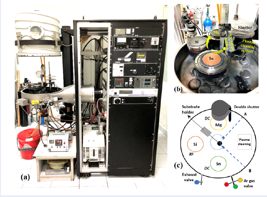
To prepare MgSiSn alloy thin films, we modified a co-sputtering configuration with three separate Mg, Si and Sn targets, which was based on the Leybold Univex-450 system (Figure 1a). The position of the targets was arranged as shown in Figure 1b and Figure 1c. The sputtering targets were located on the surface of magnetron guns which were continuously cooled at 20C by using a water chiller. Because of the lowest vapor pressure, the sputtering yield of Mg target is very high. To protect the substrate during the target pre-sputtering process, double shutters were designed. The lower shutter covered the Mg target surface, while the substrate was shielded by the upper shutter. The substrate was attached on the holder which rotates around a centered axis with a rotational angle of ~270C (from A to B and vice versa). The holder could rotate continuously with controllable angular velocity. The three magnetron guns were 15-cm equidistant from each other and 10-cm equidistant from the rotation axis. The sputtering power of each target and the angular velocity of the substrate holder were the most important parameters which affected the uniformity and composition of the MgSiSn thin films. In this initial study, the investigation was focused on changing the sputtering power of each target, thus the angular velocity was fixed at 0.375π rad/s during the deposition process.
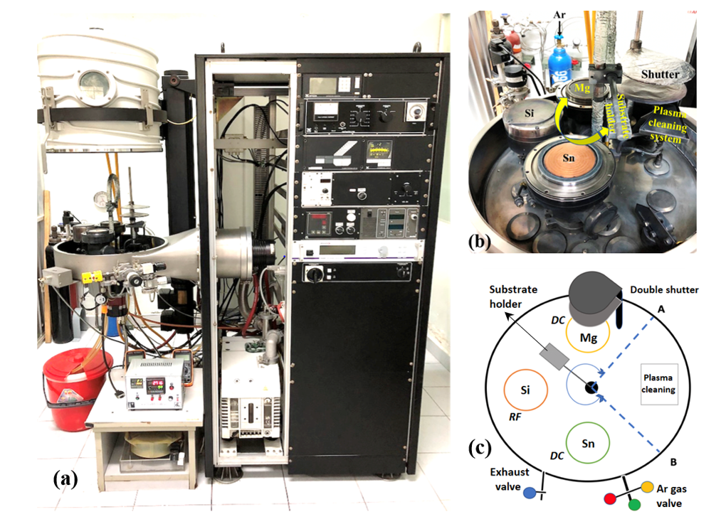
Design of magnetron co-sputtering configuration: (a) Leybold Univex-450 (Germany) sputtering system with high-speed turbomolecular vacuum pump station; (b) and (c) magnetron configuration and targets arrangement in the vacuum chamber. The three targets are equidistant from each other and from the rotation axis of the substrate.
Initial results of the MgSiSn thin films
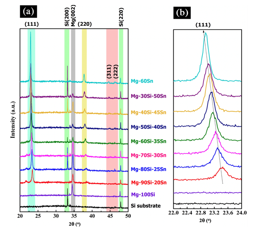
XRD patterns of the MgSiSn thin films deposited with different Si and Sn sputtering powers: (a) in large scale 2θ = 20 – 50o, and (b) in small scale 2θ = 22 – 24o. The sputtering power of Mg target is constant, whereas the power of Si target decreases from 100 W to 0 W, and the power of Sn increases from 0 W to 60 W.
Figure 2 shows the crystalline structure of the MgSiSn thin films. There are two peaks at 33.18 and 47.92 which belong to the (200) and (220) plane of the Si substrate, respectively. A clear peak located at ~34.50 is found to be the (002) plane of metal Mg phase (JCPDS 35-0821). The existence of a separate Mg phase reflects non-uniform stoichiometry or excessive Mg content in the films. This phenomenon was also reported by Zhang’s work7. More importantly, it is seen that almost the samples tend to form cubic anti-fluorite-type structure with characteristic crystalline planes, such as (111), (220), (311) and (222)8.
Based on the XRD results, the good stoichiometry and low excessive Mg phase can be obtained in the MgSiSn thin films, if the sputtering power of Si and Sn targets are lower than 60 W and higher than 35 W, respectively. Among them, the representative Mg-50Si-40Sn sample is chosen to investigate morphological and thermoelectric properties.
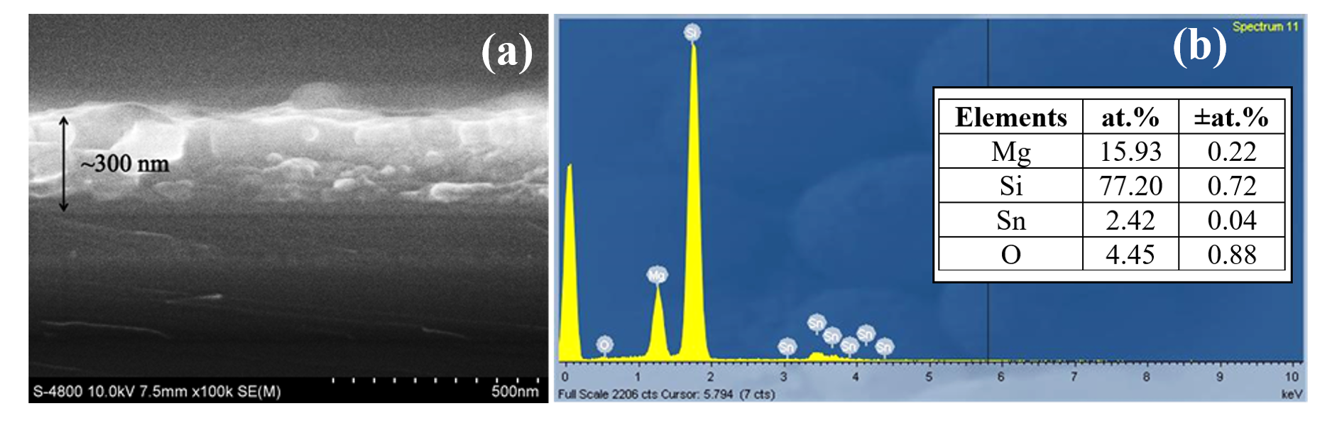
The morphology analysis of the Mg-50Si-40Sn thin film: (a) cross-sectional FESEM image, and (b) EDS elemental quantitative result. The obtained film thickness are about 300 nm, whereas the O composition might be from contamination.
Figure 3 shows the cross-sectional morphology and chemical composition analysis of the Mg-50Si-40Sn thin film. From the FESEM image, the thickness of the film is determined, approximately 300 nm. No layer separation is observed, which suggests good incorporation of the Mg, Si and Sn contents in the alloy structure. The elemental composition of the film is also checked and listed in the inset table. The EDS result indicates the successful deposition of the alloy MgSiSn film.
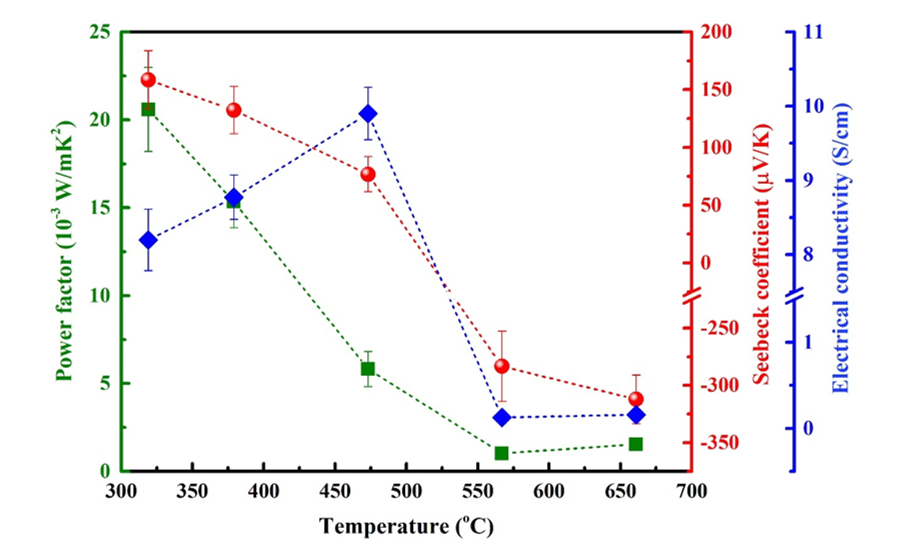
Thermoelectric parameters (electrical conductivity, Seebeck coefficient and power factor) of the Mg-50Si-40Sn thin film in the temperature range of 300 – 675 K.
Figure 4 shows some typical thermoelectric parameters (electrical conductivity, Seebeck coefficient and power factor) of the Mg-50Si-40Sn thin film. At a lower temperature than 473 K, the electrical conductivity of the films is high, which is highly-degenerated semiconductor behavior. When temperature increases more than 473 K, the electrical conductivity of the films decreases strongly, simultaneously, the value of Seebeck coefficient tends to be more negative. The thermoelectric power factor, PF = Sσ, where S is the Seebeck coefficient and σ is the electrical conductivity. The high PF value means the possibility of generating high voltage and power of thermoelectric materials when there is a temperature gradient. As a result, the highest power factor of PF ~20.5×10 W/mK corresponding to the Seebeck coefficient of S ~159 µV/K and the electrical conductivity of σ ~8200 S/cm can be observed at ~325 K.
DISCUSSION
Another proof for the formation of MgSiSn alloy is the detection of Mg, Si and Sn contents in the films, as shown in Figure 3. A problem, however, is that the composition ratio of Si is very high. It can be due to the contribution of the signals from the Si substrate. Therefore, other materials will be used as a substrate in the future studies. In addition, the O content may come from residual gas in vacuum chamber or contamination. It is also a technique problem of this co-sputtering configuration for depositing alloy thin films, which is needed to be improved.
From the measurement of thermoelectric properties in Figure 4, the Seebeck coefficient is positive, which reflects the p-type characteristic of the film. When temperature increases, the electrical conductivity decreases strongly, simultaneously, the film transforms into n-type behavior due to a negative Seebeck coefficient. It may be due to the decrease of carrier concentration and mobility at high temperatures, which is suitable for the characteristic of the highly-degenerated semiconductor. However, the transformation from p-type to n-type behavior of the film has not been understood yet. The obtained PF value is relatively high for the MgSi-based materials, but is still lower than the other reports11, 10, 9. Consequently, from the above obtained results, the alloy MgSiSn thin films prepared by using the co-sputtering configuration exhibits some thermoelectric properties. Among them, relatively high electrical conductivity and temperature-dependent semiconductor behavior of Seebeck coefficient are interesting. It is believed that the thermoelectric properties of the MgSiSn thin films can be enhanced by optimizing conditional parameters of the co-sputtering configuration.
CONCLUSION
In conclusion, the three-target co-sputtering configuration shows the possibility of successfully preparing alloy MgSiSn thin films with good adherence on Si substrate. The composition, stoichiometry, crystalline structure and thermoelectric properties of the films can be controlled through adjusting the power sputtering of each target. The typical 300 nm-thick MgSiSn film deposited at 30 W of Mg target, 50 W of Si target and 40 W of Sn target exhibits the p-type semiconductor behavior with the Seebeck coefficient of S ~159 µV/K, the electrical conductivity of σ ~8200 S/cm and the power factor of PF ~20.5×10 W/mK at ~325 K. The result suggests that the as-deposited MgSiSn thin films have some potential thermoelectric characteristics, which can be improved more significantly in the next studies.
LIST OF ABBREVIATIONS
σ: Electrical conductivity
EDS: Energy-dispersive X-ray spectroscopy
MgSiSn: Magnesium tin silicide
PF: Power factor
S: Seebeck coefficient
FESEM: Field-emission scanning electron microscopy
XRD: X-ray diffraction
COMPETING INTERESTS
The authors declare that they have no competing interests.
AUTHORS’ CONTRIBUTIONS
All authors of this manuscript have contributed to the work and approved contents of the final version.
ACKNOWLEDGMENTS
This research is funded by the University of Science, VNU-HCM, under grant number T2018-38.