

Design of a Multigate Field Effect Transistor-Based Adder for an Adaptive Filter in an Electroencephalogram Signal Analysis System
- KIT- KalaignarKarunanidhi Institute of Technology
- T. John Institute of Technology
Abstract
Various noises and artifacts affect EEG (electroencephalogram) signals and should be removed for effective diagnosis and treatment. The adaptive filter is designed using adders, multipliers and delay elements. In this paper, the design of the adder is presented. The adders form the foundational block of all arithmetic and computational processes of biomedical systems. They form the parts of filters, multipliers and transform units. The Fourier transform used in biomedical analysis uses adders as their basic elements. This work proposes a gate diffusion input (GDI) logic-based design using multigate FET transistors, namely, FinFET. The problem of a dedicated power supply and leakage current during static operation is eliminated in this work by proposing FinFET-based GDI logic. The proposed implementation was compared with existing methods on the basis of energy, power and delay. Implementation was carried out using 32 nm CMOS and FinFET technology. Predictive technology models were applied for the implementation.
INTRODUCTION
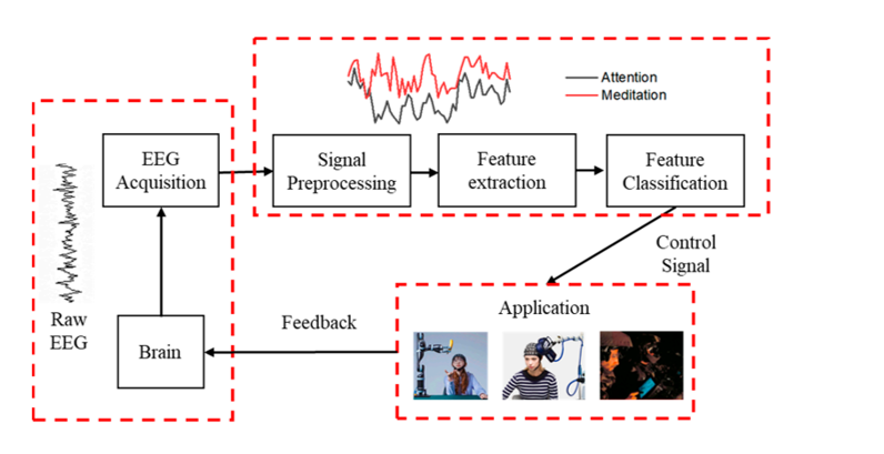
In biomedical systems, for the diagnosis of brain-related problems, electroencephalogram (EEG) signal analysis is used. The EEG signals acquired from scalp electrodes are affected by various noises. The acquisition unit should be designed to provide high amplification, accuracy and low noise. Electrodes made of Ag/AgCl were used for the acquisition process. The frequency range is from 1 Hz to 30 Hz. The cost should also be less. The preprocessing unit plays a vital role in amplification and filtering. Electrode usage is a complex process and time-consuming process that is highly prone to noise, such as baseline wandering and other noise. Figure 1 shows the EEG system with all the components. It includes acquisition, preprocessing and decision-making blocks. The analog-to-digital converter blocks are sensitive, and they determine the diagnostic performance accuracy.

Various components of the EEG acquisition system
The adaptive filters were part of the signal preprocessing and feature extraction blocks (Figure 1). Adders and multipliers were used as circuit elements in biomedical system integration using digital signal processing (DSP). Various DSP processors have been used for EEG signal processing. However, a dedicated circuit or integrated chip will be efficient. One such approach is designed in this work, where the adders for the adaptive filter are designed. Since multipliers contribute to the critical delay of the system, adders, which are the building blocks of multipliers, need attention. In addition, due to the slow development of battery technology, new circuit methods are needed. Several adaptive filters have been designed in the literature, such as LMS and RLS. The advantages of adaptive filters are that they are suitable for use in real-time settings and can process biomedical signals even in nonstationary environments. Compared with other types of filters, adaptive filters are easy to implement in hardware.
FINFET BASICS
Three-dimensional structures using fins between the source and drain provide better performance through their advanced structures. The design structure provides more space for the current to flow. (see Figure 1). Leakage is eliminated by the control of the channel through gate covering. A lower threshold voltage is used in FinFET. It works in 3 modes: low power, shorted gate and independent gate.

Device diagram of CMOSs and FinFETs
FinFET in SPICE BSIM-CMG models and PTM models were used in this work since there are 3D transistors, and capacitance values are more important. Microprocessors for EEG systems designed using multigate or tri-gate architectures consume less power. In memory cells, improved speed and battery usage are required for EEG systems. FinFETs are fabricated using front-end-of-line (FEOL) fabrication technology. The other technologies used were assembly and BEOL (back-end-of-line). In section 2, a literature survey is presented, followed by the background methodology in section 3, the proposed method in section 4, and the results and discussion in section 5. Finally, concluding remarks and references are presented.
LITERATURE REVIEW
Adaptive filters play an important role in the removal of noise from signals. The development of the adaptive filter requires several techniques, such as bit reduction methods and multipliers, as discussed by Vojin G. Oklobdzija and David Villeger 1. The structure reduces the irregular bit arrival. Developing modules from the 1-bit adder cell optimizes the design, but complex work cannot be done, as addressed by Ahmed M. Shams et al. 2. In certain designs, XOR gates are avoided, such as in the work by Mehrdad Maeen et al. 3. The 1-bit full adder cell designed in a 180 nm CMOS is better in that technology but suffers from leakage at lower technologies. A 90 nm adder was designed by Sohan Purohit and Martin Margala4. They presented the design in split-path data-driven dynamic logic. The leakage current affects the power consumption of CMOS devices and their circuits, especially when stacked, as described by Raghvendra Singh and Shyam Akashe5. The power can be further reduced in these circuits using power gating techniques. These techniques, when incorporated in larger computational blocks such as ALUs, have advantages, and adders were reported by Rachit Patel et al 6. The ALUs in CMOSs are faster, but they suffer from lower power consumption due to leakage current. However, replacing adders will reduce the delay due to RC components. Mirror adders, low-area adders, branch-based logic and pass transor logics have been designed7, 8. At 180 nm, Mariano Aguirre-Hernandez and Monico Linares-Aranda9 developed adders in CMOS technology. Other adders have also been developed using hybrid circuits and gate diffusion input (GDI), a new technique for low-power digital combinatorial circuit design10, 11. Gate diffusion logics have been used in the design of adders and other combination circuits 12, 13. The full swing gate diffusion input (FS-GDI) methodology was found to be effective when low-power circuits are required14, 15. Senthil Kumar et al. (2019) used FinFET with a self-controllable-voltage-level (SVL) circuit for opamp design. CNTFET- and FinFET-based DWTs were also designed for the DWT architecture. Ravindrakumar et al. (2017) used adaptive filters for fetal ECG extraction. In that work, several adaptive filters were designed. Gupta et al. (2020, 2021) designed FinFET-based architectures for DWT architectures. A similar type of FinFET-based design was developed by Senthilkumar et al. (2019). Ravindrakumar and Nithya (2012) designed a system for ECG signal processing. Leakage is eliminated by several means using FinFET logic circuits16, 17, 18.
Research Gaps Identified: The main problem in the existing CMOS technology is the power consumption due to leakage current, slow computation and low accuracy. These problems can be addressed using new technology that can reduce power consumption. The speed of operation is improved, and more computations are performed. When EEG signal analysis concerns, the design should involve filtering block optimization. The filters are computing blocks that use time, frequency or time-scale methods. In this work, adaptive filters, which have a very high rejection ratio and good extraction of information, were chosen. PTL design methods face problems due to the low swing of outputs. The pass transistors provide less of a voltage drop. When the device works in the subthreshold region, swing decreases, and the delay increases. Additional buffers increase the area of the system. The skew and jitter, on the other hand, increase due to buffers.
BACKGROUND METHODOLOGY
Figure 3 shows the GDI method and its various nodes of ‘N’, ‘P’ and Gate. Arbitrary biasing is possible at the connection between the N and P connected with the bulks of nMOS and pMOS, respectively. There are few relationships between N and P, N input-VDD and P input=0. Direct polarization occurs between the diodes, static power dissipation occurs, and V ~ 0.5V.

GDI basic cell
PTL design methods face problems due to the low swing of outputs. The pass transistors provide less of a voltage drop. The F1 function choice in GDI eliminates this problem, and the voltage level is V. The GDI has a transient analysis similar to that of CMOS. Here, the nMOS diffusion is given with a step signal.
FULL ADDER TOPOLOGIES
The variousfull adder circuit types are shown in Figure 4. The types are C-CMOS adder cells, b) TG-pseudo adder cells and c) TG adder cells. The first circuit provides full swing lmost to the V and -V.

a) C-CMOS adder cell b) TG-pseudo adder cell c) TG adder cell
The high-speed PseudonMOS full adder cell with 14 transistors, as shown in Figure 4b, has more static power consumption. The circuit avoids a zero voltage drop at the output node. The circuit increases the area of the circuits. However, it has low power consumption.
These designs work on EEG multiinputs, which are complex signals. Since EEGs have more harmonics and event potentials, it is very challenging to reduce the error signal and improve the convergence behavior. Power spectral analysis provides a clear picture of the frequencies in the signal and its amplitude. The amplitude will be in microvolts. The characteristics are rhythmic with constant frequency, arrhythmic without a stable frequency and dysrhythmic.
PROPOSED SYSTEM
In this work, we developed and implemented a GDI-based design using multigate technology. The problems in CMOS and other filters are addressed, and we arrive at an effective circuit. The proposed design eliminates threshold voltage loss, is less complex and can achieve high speed even in cascade operation. In this work, FinFET-based adders were designed and implemented for the RLS DCD architecture. For EEGs, the signal power is low, and a conventional adaptive filter will find it difficult to adapt to varying multimodal error surfaces.
Dichotomous Coordinate Decent (RDR) Block Algorithm
Figure 5 shows the block RLS Dichotomous Coordinate Decent (DCD) architecture. This algorithm uses an adaptive filter to update the weights in a blockwise and clockwise manner. The buffers store the intermediate results. In every clock cycle, the updation is performed from the output of the error values. There is less sampling of biomedical signals, so the block of data contains the maximum amount of information. The averaging of the block of data is performed so that the medical data information is not affected. The mathematical form of the block RLS DCD algorithm. Xo, x1, and xn are input samples. W1, w2, and wn are weight values.

Block RLS DCD Adaptive Filter
The block RLS algorithm-based adaptive filter is implemented using buffer blocks, as shown in Figure 5. The implementation shown in Figure 5 consists of registers or memory units to store the coefficients, weighted units, adders and multipliers. These units are suitable for real-time implementation. The unit is autonomous, and no manual control is needed. The updation unit calculates the weight values, which are subsequently updated based on the error inputs. Buffers are placed in all units to store the temporary data. The tap count determines the number of multipliers in the system. The step size determines the convergence rate of the adaptive filters. The step size is variable based on the signal. Here, the steady-state error and convergence rate are optimized using the step size variation. y[n] and d[n] are convolved, and errors are produced. Based on the error signal, the weights are updated. The subtractor is also an adder with one of the inputs: the 2’s complement data. The implementation of the FIR using multipliers is found to be efficient. The critical paths can be optimized by using pipelining stages.
PROPOSED FULL ADDERS IN GDI FOR THE RLS DCD ALGORITHM
Here, the proposed full adder design featuring a GDI cell for an adaptive filter RLS DCD is presented. The proposed design has full swing logic. The sum and carry are presented by the Boolean expression in equations 5 and 6.
Sum= A XOR B XOR Cin (5)
Cout = A AND B + B AND Cin + A AND Cin (6)
The GDI cells for AND, OR and XOR are shown in Figure 6. As shown in Table 3.1, GDI logic can work according to different logics. In addition, for input combinations of all ‘0’s, the current is limited. CMOSs already have issues in this regard. FinFET will be the right choice for this application.

Circuits of the (a) XOR gate, (b) OR gate and (c) AND gate
Implementation of the adder circuit
The full swing gates were suitable for the GDI full adder unit for EEG signal processing. The performance was improved by using a FinFET device, where the leakage current was reduced and the full swing was confirmed. A swing restoration block is not needed. In EEG signal processing, the amplitude of the input is less, but it can be rectified by using the amplifier stage in the acquisition unit. The filtering unit removes the noise present in the EEG signal. Normally, an EEG recording of cognitive behavior requires a proper filtering unit for noise removal.
Design 1 using GDI is shown in Figure 7.

Circuit for design 1 using GDI
The full swing configuration expressions are given in Eqs. (7) and (8):
Sum= Cin (A XOR B) +Cin (A XNOR B) (7)
Cout = (A XOR B)Cin + (A XOR B)A (8)
The intermediate result is the XOR unit.
Design 2 using GDI is shown in Figure 8. This design uses multiplexer, XOR, OR and AND gates.

Design 2 Proposed full adder
Sum= A XOR XOR Cin (9)
Cout = Cin (A AND B) +Cin (A OR B) (10)
Design 3 using GDI with an intermediate XOR gate is shown in Figure 9.
Sum= A XOR B XOR Cin (4.7)
Cout = A AND B + (A XOR B)Cin (4.8)

Design 3 Proposed full adder
The ASIC-based implementation is advantageous compared to the FPGA. Here, analog units can be developed. The supply voltage can be varied as per the requirements. GDI logic is difficult to implement in FPGAs. The disadvantage of the proposed method is that at high noise levels, the output swing may decrease. In addition, the coefficient update block is updated according to the signal-to-noise ratio. Therefore, at a high noise content, the increase is slower as the convergence rate increases. This can be optimized using techniques that can optimize the coefficient updating unit.
RESULTS AND DISCUSSION
The predictive technology model files from TSMC were used. These model files have parameters for 32 nm technology in CMOS and FinFET devices. The model files have physical and electrical device details, which will be fetched by the simulator to make the original device. A schematic diagram of the full adder-based Design1 circuit is shown in Figure 10. The inputs used in design1 are A, B, and C, and the outputs for this circuit are sum and carry. Here, the full adder used is the GDI full adder.

Proposed full adder-based Design1

Proposed full adder-based Design2
A schematic diagram of the full adder-based Design2 circuit is shown in Figure 11. The inputs used in design2 are A, B, and C, and the outputs for this circuit are sum and carry.

Proposed full adder-based Design3
A schematic diagram of the CMOS full adder-based Design3 circuit is shown in Figure 12. The inputs used in design3 are A, B, and C, and the outputs for this circuit are sum and carry.

Proposed FinFET full adder-based Design1
A schematic diagram of the FinFET full adder-based Design1 circuit is shown in Figure 13. The inputs used in design1 are A, B, and C, and the outputs for this circuit are sum and carry. Here, the FinFET full adder used was the 32 nm GDI full adder.

FinFET full adder-based Design2
A schematic diagram of the FinFET full adder-based Design2 circuit is shown in Figure 14. The inputs used in design2 are A, B, and C, and the outputs for this circuit are sum and carry.

FinFET full adder-based Design 3
A schematic diagram of the FinFET full adder-based Design3 circuit is shown in Figure 15. The inputs used in design3 are A, B, and C, and the outputs for this circuit are sum and carry. Here, the FinFET full adder used was the 32 nm GDI full adder.
Analysis of SwingRestoring as per Figure 11 to Figure 15
Figure 10-Figure 12 and 13-15 show the different design implementations using CMOSs and FinFETs. The circuit shows buffer units that eliminate swing restoration in GDI circuits. In addition, as shown in
Power analysis of the CMOS and FinFET full adder
|
CMOS 32_nm Design |
FinFET 32_nm design | |||||||
|
AVERAGE POWER |
PEAK POWER |
AVERAGE CURRENT |
PEAK CURRENT |
AVERAGE POWER |
PEAK POWER |
AVERAGE CURRENT |
PEAK CURRENT | |
|
FULL ADDER DESIGN1 |
7.06E-05 |
1.74E-02 |
-3.37E-05 |
1.04E-01 |
4.10E-07 |
3.36E-07 |
-4.10E-07 |
-3.73E-07 |
|
FULL ADDER DESIGN2 |
1.05E-03 |
5.82E-01 |
-7.85E-05 |
8.5621 |
4.48E-07 |
3.66E-07 |
-4.48E-07 |
-4.07E-07 |
|
FULL ADDER DESIGN3 |
8.10E-04 |
4.76E-01 |
-4.61E-05 |
4.0212 |
4.47E-07 |
3.65E-07 |
-4.47E-07 |
-4.06E-07 |
Power delay analysis of the full adder
|
power delay product | |||
|
CMOS(45_nm) |
CMOS(32_nm) |
finFET(32_nm) | |
|
FULL ADDER DESIGN1 |
6.41E-14 |
8.17E-14 |
1.84E-15 |
|
FULL ADDER DESIGN2 |
6.41E-13 |
5.60E-13 |
1.98E-15 |
|
FULL ADDER DESIGN3 |
5.71E-13 |
6.65E-13 |
2.02E-15 |
PDP (power delay product) = average power * average delay.
CONCLUSION
In this paper, FinFET-based adder circuits for an RLS DCD adaptive filter are designed and implemented. The design was used in the EEG signal processing unit. In biomedical signal processing, more adaptive filters are required for noise. Currently, since most devices are battery operated, dedicated circuits that can provide less power are needed. In conventional methods, CMOSs, which suffer from leakage current, are used. In this work, the GDI logic is designed in a finfet, which provides less power and fast operation. The full swing XOR, AND and OR gates for functions F1 and F2 are used. This eliminates the threshold voltage problem. Buffers are introduced to increase the driving capability. This also provides low power by using FinFET devices. The SPICE simulation tool at 35 nm was used. The performances of various circuits are compared. The implementation was carried out in Synopsis using CMOS and FinFET PTM models.
In the future, the proposed method can be implemented using field programmable gate arrays and signal processors. An embedded system will be implemented for the acquisition units to control and transmit information to remote places. IoT-based design will be a focus of future research.