

The effect of content and thickness of chitosan thin films on resistive switching characteristics
- Faculty of Materials Science and Technology, University of Science, Ho Chi Minh City, Vietnam
- Laboratory of Advanced Materials, University of Science, Ho Chi Minh City, Vietnam
Abstract
Introduction: Nowadays, a resistive switching memory using biological, transparent, and environmentally friendly materials is appreciated as the tendency of science and technology, especially in the field of electronic devices. Chitosan (CS), having dominant characteristics such as non-toxic, biocompatible and large capacity, plays as a switching medium in resistive random access memory devices (RRAM).
Methods: In our study, CS film was fabricated onto a commercial substrate (FTO) using a simple spin coating method, and the top electrode (Ag) was deposited by a direct-current sputtering technique.
Results: The Ag/CS/FTO devices shown the bipolar switching behavior when applying sequence voltage from -1.5 to 2V with the set process in the negative bias and the reset process in the positive bias. The content (0.2, 0.5, and 0.8 wt%) and thickness (100, 300, 500 nm) of chitosan film significantly affect the resistive switching performance. The devices with 0.5 wt%/v concentration and 300 nm-thickness of CS have shown better efficiency than the others with endurance over 100 sweeping cycles and ON/OFF ratio at ca. 2x10 times.
Conclusions: It is found that the chitosan material has a large potential candidate for applications in optoelectronic devices.
INTRODUCTION
Recently, chitosan (CS), one of the potential biopolymer materials, has been promoted researches to apply in many areas because of its highlight characteristics such as non-toxic, environmentally friendly, and large capacity 1, 2. CS extracted from chitin, which is derived from shrimp, lobster shells, crab, krill, mushroom, etc. is available in nature with large reserves 3. CS has been applied in many fields such as biomedical, drug delivery, and photocatalysis. More recently, chitosan has been employed as an insulator layer in resistive switching memory devices. This memory is expected to replace the traditional memory technologies due to its advantages such as low cost, high speed, long retention, and fast write/read speed 4, 5, 6, 7, 8. Besides, chitosan plays as a dielectric layer in transistors 9, 10.
On the other hand, the influence of film thickness on the characteristics of the resistive switching device based on organic materials has been reported by different groups 11, 12. A device of fullerene-derivative [6,6]-phenyl-C butyric acid methyl ester mixed with inert polystyrene matrix has the threshold switching voltage and ON/OFF state current ratio depending on the film thickness 13. A Poly( N-(N,N'-diphenyl-N'-1,4-phenyl)-N,N-4,4'-diphenylene hexafluoroisopropylidene-diphthalimide) with a thickness of >15 to <100 nm exhibits the write-one-read-many-times (WORM) and ON/OFF ratio ~ 10 while 100 nm-thick film shows dynamic random access memory (DRAM) with ON/OFF ratio ~1014. Similarly, using -conjugated polymer, poly(diethyldipropargylmalonate), it is observed stable WORM at 30 nm-thick film and DRAM at 60-120 nm-thick film 15. A device based on a polymethacrylate with depend azobenzothiazole shows FLASH memory or WORM behaviors according to the film thickness 16. Besides, the thickness of inorganic thin films also influence on the resistive switching performance of GdO17, AlN 18, amorphous BaTiO11. From these reports, it is learned that the thickness of the insulator layer plays an important role in resistive switching characteristics and behaviors. However, the investigations related to thickness influence are not comprehensive understanding, especially on biopolymer.
Therefore, in this study, we fabricated the RRAM devices using CS as a switching layer in Ag/CS/FTO structure and investigated its resistive switching behavior. Furthermore, the effect of content and thickness of chitosan thin filmson the performance of a memory device was explored in this study.
EXPERIMENTAL PROCEDURES
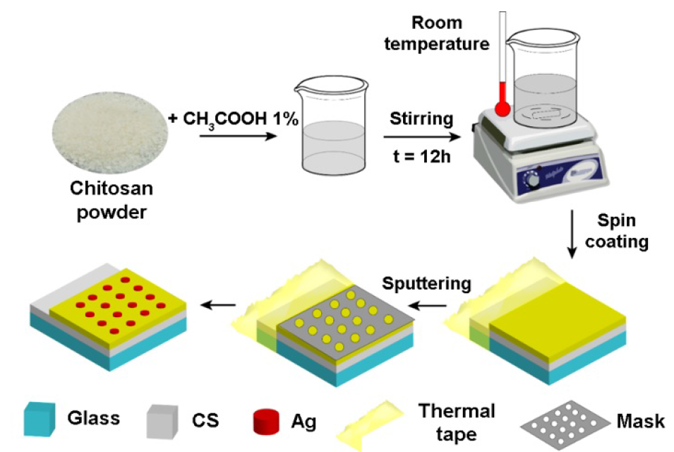
The RRAM device with Ag/CS/FTO structure using CS as a switching layer was prepared by using the schematic presented in Figure. 1. Firstly, CS powder (99.99% in purity, Acros) at different weights of 0.2, 0.5 and 0.8 g was dissolved in 100 ml acetic acid solution (1.0 wt%) to form 0.2, 0.5, and 0.8 wt/v CS solutions, respectively. The mixture was continuously stirred at room temperature for half a day. Then, it is used to fabricate CS thin film by spin-coating at 2000 rpm for 30 seconds on the FTO substrate, which has covered edge position by taping to guard electronic characteristics of FTO. The thickness of the CS thin film was controlled by the number of spin-coating. Herein, we fabricated devices with CS film thickness around 100, 300, and 500 nm. Finally, circular Ag top electrodes were deposited by direct-current sputtering technique via a shadow mask with a diameter of 100 nm.
The crystalline features of the chitosan powder and thin films were conducted by using an X-ray diffractometer (XRD) with Cu Kα radiation (λ = 0.154 nm) (D8 Advance, Bruker) while Fourier-transform infrared (FTIR) spectroscopy (Vertex 70, Bruker ) was used to identify chemical vibrational peaks in the powder and thin film patterns in the mid-infrared range of 400–4000 cm. The surface morphology of the CS thin films was observed by a scanning electron microscope (SEM) (S4800, Hitachi). Finally, Current–Voltage (I–V) measurements were measured using a Keithley 2400 system and a probe station system. The voltage sweep range for the I–V measurements was 0 V +2 Và 0 V -1.5 V 0 V. The bottom electrode (FTO) was biased, and the top electrode (Ag) was grounded. The endurance characteristic of the device has been tested using voltage sweeping conti uously 100 cycles on the device, then calculating the resistance at HRS and LRS corresponding to current and reading voltage @ 0.5 V. The resistance ratio was calculated from the division of resistance at HRS to resistance at LRS.
The schematic for the fabrication of Ag/CS/FTO structure. Chitosan film was coated onto the FTO substrate from aqueous solution. The Ag film was deposited as a top electrode using a sputtering method and a shadow mask.
RESULTS
Figure 2 shows the results of XRD patterns for the chitosan material in powder and thin film. For CS powder, the prominent peak is observed clearly at around 2q = 20°, which is corresponding to the characteristic crystalline of (100) plane in CS material 19. However, the other peak of chitosan at approximately 2q = 10° assigned to the (020) plane does not appear in this pattern. It may be due to the chitosan degree of deacetylation of pristine powder. The crystalline structure of CS powder can be explained due to the periodic characteristics of molecular structure with the intermolecular hydrogen bonding 20. The CS thin film exhibits a broad peak and low intensity at about 2q = 22°. The intensity decrease and the position shift in the thin film compare to its in powder may be due to the interaction of acetic acid and the CS chains.
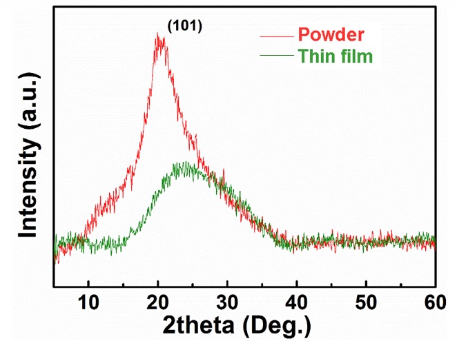
XRD patterns of chitosan in powder and thin film. The diffraction angle of 2theta was measured from 5 to 60o. The chitosan film was coated on the soda-lime glass substrate.
Figure 3 shows the FTIR spectra in the range from 500 to 4000 cm of CS powder and CS thin film, which are studied to determine the vibration of functional groups and chemical bonding.Both patterns of powder and thin film exhibit characteristic peaks at the same wavenumbers, but the vibrational peaks in powder are more inten ively comparing to their in the thin film. These peaks are similar observed in chitosan as the previous reports 21, 22, 23. A broad and high-intensity band at around 3450 cm are corresponding to overlaps of N-H and O-H stretching vibrations 24. For the band lower than 3000 cm, the vibration exhibits the stretching vibration of C-H sp (~2900 cm), C-H bending (1365 cm), and C-O-C bridge stretching at 1082 cm22. Besides, we can recognize the N-H bending vibration (1615 cm) 23, 24, 25. According to this result, we can recognize that the suitable features between powder CS and the thin film CS with characteristic peaks were observed at the same wavenumber.

FTIR spectra of chitosan powder and thin film. The 100 nm-thick chitosan film was coated onto a silicon substrate.
The cross-section SEM images were surveyed to investigate the uniformity and thickness of CS film on the FTO substrate, as shown in Figure 4 at the scale of 1.00 um and 500 nm. We can observe clearly that the interface position between FTO substrate and CS thin film is coated evenly with around 300 nm thickness. Besides, this result is in good agreement with XRD records with an amorphous state of CS thin film.

Cross-section SEM images of chitosan film on the FTO substrate. The high roughness surface and less dense structure film have been observed.
The resistive switching behavior of the Ag/CS/FTO structure is evaluated by applying the continuous voltage sweeps, in which the top electrode (Ag) and the bottom (FTO) were biased and grounded, respectively. Herein, we randomly selected the I-V characteristic of the device at 0.5% wt/v and 300 nm thickness of the CS layer to analyze. We proceeded voltage sweeps from 0 V –1.5 V 0 V 2 V 0 V to investigate the RS characteristics. The results indicate that bipolar RS characteristics were observed in the I–V curves with a linear and semi-logarithmic plot, as seen in Figure 5 A-B. Initially, this device show a pristine state with high resistance state (HRS), then the current gradually increase and abruptly increases to ~10 A until voltage a proaches to -1.24 V. This transition from the HRS to a low-resistance state (LRS) indicates that the “SET” process of devices or “writing” process of the digital memory device. To prevent the sample from permanent breakdown, current compliance of 500 mA is usually needed during the sweeping process 26. This state maintains in the voltage range of –1.5 to 0 V. After that; the voltage applies from 0 to 2.0 V, the device continues to hold LRS, then switches to HRS at the voltage of 1.26 V and the current drops rapidly to ~ 2 x 10 A. This transition is called “RESET” process of devices or “ERASE” process of the digital memory device. The HRS retains when sweeping back to 0 V again. The above I–V characteristics indicate that the Ag/chitosan/FTO device shows reversible bipolar resistive switching behavior. The device switches from the HRS to LRS at the negative bias and back from HRS at the positive bias. The operating voltages of V –1.24 V and V 1.26 V are relatively low, and the ON/OFF ratio was larger than 20 times. These characteristics can be considered for electronic memory device applications.

The I–V characteristics of the Ag/chitosan/FTO structure. (a) The linear plot and (b) the semi-logarithmic plot in the sweeping voltage of -1.5 V
For the RRAM structure, the dielectric CS layer exhibits an important role in the switching behavior of the structure. In this part, we have investigated the effect of CS content in switching behavior in the same structure. Herein, we have fabricated devices with different CS concentration of 0.2, 0.5, and 0.8 %wt/v. The I-V characteristics and endurance of 1 – 100 sweeps of corresponding patterns are depicted in Figure 6 A and B. The results indicate that all of it shown the bipolar resistive switching behavior. However, the effect of 0.2 %wt/v of CS into the device does not maintain and starts fades away when reaching 80 cycles. At 0.5 wt/v of CS, the resistive switching hold on with a more stable and higher ON/OFF ratio (~ 2x10) than those of 0.8 %wt/v (Figure 8 A). This result indicates that the content of CS in the Ag/CS/FTO structure is one of the significant factors, which influence the reproductivity and ON/OFF ratio in resistive switching properties of devices.

The I-V characteristics of the Ag/chitosan/FTO structure with different concentrations of CS. (a) The semi-logarithmic plot of I-V curve and (b) endurance of 1st-100th cycles corresponding to 0.2%, 0.5, and 0.8 %wt/v content of CS.

The I-V characteristics of the Ag/chitosan/FTO structure with different thicknesses of CS. (a) The semi-logarithmic plot and (b) endurance of 1st-100th cycles at 100, 300, and 500 nm thickness of CS film.
As presented above, the device with 0.5 %wt/v CS content showed better switching behavior than the others. Thus, we combine this content with CS thickness of 100, 300, and 500 nm to investigate their effect on the resistive switching behavior. The I-V characteristics and endurance of corresponding thickness are presented in Figure 7 A and B. The device with 100 nm-thickness chitosan tends to reduce the ON/OFF ratio follow the cycling bias while 500 nm-thickness of chitosan has a resistance ratio slightly lower than that of 300 nm (Figure 8 B). This result implies that the device with 300 nm thickness of the CS layer and 0.5% wt/v exhibits the largest ON/OFF ratio and the most stable compared to the others.

The resistance ratio of the Ag/chitosan/FTO structure. (a) With CS concentration of 0.2, 0.5 and 0.8 wt%, With CS thickness of 100, 300 and 500 nm.
DISCUSSION
The resistive switching characteristics of the Ag/chitosan/FTO device in this study show the non-volatile random access memory with bipolar behavior (Figure 5), which is consistent with the previous reports based on chitosan material 8, 27. The operating voltages of our device are similar to their devices with under 3 V. It exhibits the advantages of low power consumption in electronic devices. The ON/OFF resistance ratio is the same as the group [8] with several tens but lower to the other one 27. In our device, we use undoped chitosan as an insulator layer in the capacitor structure, while Ag-doped-chitosan, Mg-doped-chitosan layer are used in other studies.
The chitosan concentration influences on the fluctuation of current-voltage curves of devices after 100 sweeping cycles. Under the same operating voltages, current compliance, and film thickness, devices exhibit the largest variations at 0.2 wt%, then following by 0.7 wt%, but they are the most stable at 0.5 wt%. The different concentrations of chitosan in solution are related to the dispersion level of polymer chains in the solvent. In the acetic acid, chitosan may protonate and form polycation chitosan. It may influence the electrical property of the chitosan layer, or the resistance at HRS and LRS, and vary the ON/OFF ratio. In our research, the suitable concentration of chitosan is about 0.5 wt% in 1.0 wt% acetic acid (Figure 8 A). The effect of chitosan concentration has been investigated in bioapplication 28, 29, The changes in crystallinity, morphology, degree of the acetylation of chitosan, which was sonicated in various concentration of acetic acid have also reported 30.
The effect of chitosan thickness is strongly on the ON/OFF ratio during 100 cycles (Figure 8 B). At the thickness of 100 nm, the ON/OFF ratio approaches 10 at the first several cycles but then decrease promptly with tens of cycles due to the increment of resistance at LRS. This decrease of ON/OFF ratio completely disregards in the 300 nm – thick – film with the stable resistances at both HRS and LRS. In the 500 nm – thick – film, the resistance at HRS slightly decreases, leading to the pretty reduction of ON/OFF ratio in this sample comparing to the 300 nm – thick – sample. In other reports, the thickness of the insulator layer has influenced the resistive switching characteristics such as the multilevel threshold in amorphous BaTiO [11] or the ON/OFF resistance ratio in AlN material [18]. The thickness of the insulator film varies the roughness and the leakage current as well as the electrical conducting mechanism of structure [11], [18]. In our study, the 300 nm – thick – film of chitosan is applicable for memory devices.
CONCLUSIONS
In summary, we fabricated RRAM devices successfully using CS as a switching layer in Ag/CS/FTO structure. The I-V characteristic devices shown bipolar resistive switching behavior in the range of -2 ¸ 2 V. Furthermore, the influence of content and thickness of CS film on the resistive memory characteristics were investigated. Our results indicated that the RS behavior at 300 nm-thickness and 0.5 wt%/v of CS thin film was shown stable and reliable during 100 cycles and ON/OFF ratio around ~ 2x10.
Abbreviations
CS: Chitosan
FTO: Fluorine-doped Tin Oxide
HRS: High Resistance State
I-V: Current-Voltage
LRS: Low Resistance State
RRAM: Resistive Switching Random Access Memory
SEM: Scanning Electron Microscopy
Authors' Contributions
Dinh Phuc Do and Tu Uyen Doan Thi performed experiments under the supervision of Ngoc Kim Pham. Tran Duy Tap and Van Dung Hoang analyzed data. Dinh Phuc Do and Ngoc Kim Pham wrote the paper.
Conflict of Interest
There are no conflicts of interest to declare.
ACKNOWLEDGMENTS
This research is funded by Vietnam National University Ho Chi Minh City (VNU-HCM) under grant number C2018-18-27.