

All-graphene-based transparent and flexible ultraviolet photodetectors
- VKTech Research Center, NTT Hi-Tech Institute, Nguyen Tat Thanh University, 298-300A Nguyen Tat Thanh Street, Ward 13, District 4, Ho Chi Minh City, Vietnam
- Department of Materials Science and Technology, University of Science, Ward 4, District 5, Ho Chi Minh City, Vietnam
- Vietnam National University, Ho Chi Minh (VNU-HCM), Linh Trung Ward, Thu Duc District, Ho Chi Minh City, Vietnam
Abstract
The excellent electrical and optical properties make graphene suitable for transparent conductive electrodes in optoelectronic device applications. However, the lack of an energy bandgap of graphene has caused many obstacles in practical applications. To overcome this issue, graphene-based semiconductor heterojunctions have been proposed, but challenges still remain due to the chemically inert surface of graphene, which causes many difficulties in forming a junction. We have proposed an alternative strategy based on chemically modified graphene architecture in this context. This combination creates a novel platform based entirely on graphene material so that it can perfectly connect together. All-graphene-based transparent ultraviolet photodetectors comprised of a reduced graphene oxide layer and graphene quantum dots have been manufactured and tested. Under a 2 V applied voltage and 380 nm illumination wavelength, this structure has a responsivity of 2 A/W with a rise/decay duration of 100 s.
Introduction
Transparent and flexible UV sensors have sparked much attention since they are foldable, wearable, lightweight, and portable devices 1. To date, traditional ultraviolet sensor active layer materials have not been suitable for integration on flexible and transparent substrates. Low-dimensional inorganic nanostructures have been used in most flexible UV sensor research; however, their optical transparency is poor, and their manufacturing techniques and device combination are troublesome. As a result, large-scale production has been hampered. Furthermore, the nature of the soft substrate, which is very sensitive to high-temperature processes causing mechanical deformation, limits the production of transparent and flexible UV sensors. Consequently, many classic semiconductor fabrication processes are no longer feasible, or if they are, they can damage device performance. One of the most crucial elements to consider is mechanical hardness. Indium tin oxide (ITO) is typically used for the traditional transparent conducting layer. However, the ITO substrate is rigid and will deform when bent. The device’s performance suffers as a result of this issue, and the yield suffers as a result.
Due to their outstanding physicochemical properties, such as high electrical conductivity while ensuring good optical transmittance, environmental friendliness, abundance, and typically suitability for the low-temperature process, graphene two-dimensional materials have emerged as a potential candidate to replace conventional materials in the construction of the next generation of UV sensors2. However, the lack of an energy bandgap of graphene has caused many obstacles in practical applications. To overcome this issue, graphene-based semiconductor heterojunctions have been proposed, but challenges still remain due to the chemically inert surface of graphene, which causes many difficulties in forming a junction. In this study, we have proposed an alternative approach that is to combine graphene with chemically modified graphene. This combination creates a unique architecture that is totally made of graphene material and can link properly. For application, all-graphene-based transparent ultraviolet photodetectors (UVPDs) have been fabricated and investigated. The manufactured device platform is made of a chemical vapor deposition graphene transferred bottom electrode and a spray-coating of chemically modified graphene such as reduced graphene oxide (rGO) and graphene quantum dots (GQDs) that serves as an active layer. Our research reveals the enormous promise of graphene-based platforms for scalable processes, high optical transparency, and inexpensive and flexible sensors.
Experimental method
Materials synthesis and characterization
Chemical vapor deposition of graphene growth
The chemical vapor deposition approach was used to create graphene films on copper foil. Cu foil was washed with acid and DI water to remove the oxide layer and all surface contaminations and then loaded into a CVD chamber to begin developing at 1050 °C and 10 Torr pressure with a 5-minute flow of methan and hydrogen gases in a 1:4 ratio. After graphene formation, the chamber was cooled to room temperature before removing the foil. The formation of graphene on Cu foil was related to the surface-catalyzed process, implying that metal acts as a catalyst. A more in-depth look into the growing method of graphene can be found elsewhere3. The hydrocarbon molecules decompose at the metal surface, and carbon atoms diffuse into the metal. Copper is an excellent candidate for making large-area graphene films with uniform thickness due to the low solubility of C in Cu4.
Synthesis of reduced graphene oxide (rGO) dispersion
A modified Hummers method was used to make a GO dispersion from expanded graphite5. First, graphite flakes (grade 1721, Asbury Carbon) were microwaved for 10 s to expand them to 150 times their original volume. A three-liter flask with three necks was then filled with 500 mL of concentrated HSO. To cool the flask to 0 °C, it was placed in an ice bath. Expanded graphite was progressively inserted to form a suspension. Next, KMnO4 was added while the temperature was kept below room temperature. After chilling the flask, 5 L of deionized water was added after one hour of stirring. Slow addition of 50 mL of HO (30 wt%) to the solution resulted in many bubbles and a shift in hue from dark brownish to yellow. The suspension was filtered and washed four times with a 10% HCl solution and then rinsed six times with 8 L of deionized water to completely eliminate the acid, lowering the pH to 6. The GO dispersion was a paste when it was made. The concentration of GO was determined to be 1.5 wt% after drying the GO dispersion at 80 °C under vacuum for 24 hours. In this study, we employed an excessive amount of hydrazine reducing agent and a long reduction time to make a rGO dispersion.
Synthesis of GQD dispersion
A solution of 0.8 g citric acid and 0.7 g ethylene diamine (EDA) diluted in 20 mL water was used to make the GQD dispersion. The solution was transferred to a stainless-steel autoclave with a Teflon liner and a capacity of 50 mL. The autoclave was heated to the appropriate temperature of 160 °C at a rate of 1.5 °C/min and then placed in a vacuum oven for an additional 5 hours. After the autoclave had cooled to room temperature, the product was diluted with ethanol and centrifuged at 5000 rpm for 5 minutes. After discarding the supernatant, the precipitates were chosen and redispersed in distilled water. Using a UV–Vis measuring instrument, the optical characteristics of an all-graphene-based platform were examined (Edinburgh Instruments DS5). Laser Raman spectroscopy with an excitation wavelength of 632.8 nm was performed to investigate the bonding structure of the active layer. TEM (JEON JEM-2100F) and AFM were used to investigate the morphology of the samples.
Device fabrication
First, the physical growth of graphene on a copper (Cu) surface by means of the chemical vapor deposition method was spin-coated with PMMA, followed by droplets of PDMS in the transferred graphene technique. Both polymers are solidified and hardened at 110 °C. The Cu is then chemically etched with an iron chloride etchant to produce PMMA and PDMS-coated graphene. PMMA was chosen because it dissolve quickly in acetone, while PDMS functions as a passivation layer and facilitates sample handling. Following the etching process, the prepared film is washed in DI water and then removed with tweezers before being deposited on a flexible PET substrate. In this case, of study, polyethylene terephthalate (PET) is employed as the transparent and flexible substrate. After transfer to a PET substrate, heat treatment at 110 °C for 10 minutes in a furnace was carried out to guarantee complete drying and the formation of chemical bonds between graphene and the PET surface. The samples were submerged in acetone to remove the polymers and then washed with DI water before being left with graphene bonded to the PET substrate.
Second, with the use of a shadow mask and reactive ion etching equipment, the interdigital bottom electrode is created using oxygen plasma treatment. Finally, to make transparent and flexible UVPD devices, the rGO dispersion was sprayed over a bottom interdigitated graphene electrode built on a PET transparent and flexible substrate, followed by the deposition of GQDs. The layer-by-layer spray-coating of rGO and GQDs was carried out at 120 °C. All of the UVPD device construction stages are depicted in Figure 1.
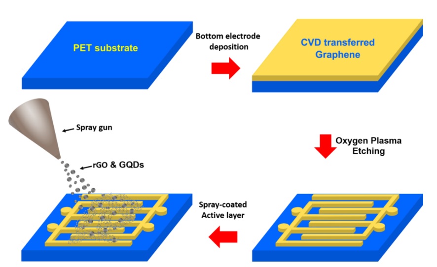
Fabrication procedure for transparent and flexible all-graphene-based UV photodetectors.
Measurement
The silver paste combined with the copper plate used to contact the two graphene electrodes of the device makes it easier to measure the photoelectric properties of the fabricated device, as illustrated in the inset of Figure 3a. The current-voltage (I-V) of UVPD devices was monitored using semiconductor characterization equipment while they were subjected to a 380 nm wavelength (LED) light source with varying power (Keithley 4200-MS Tech). To examine the device selectivity, the device responsivity was simultaneously measured as a function of the incident wavelength emitted from a xenon lamp (450 W) and Oriel Cornerstone 130 1/8 m monochromator.
Results
Figure 2(a) shows the TEM images of synthesized GQDs, and the inset figure depicts its diffraction pattern. As shown in Figure 2(a), the synthesized GQDs have a size homogeneity, with diameters ranging from 5 to 7 nm. As revealed by the electron diffraction pattern, the as-synthesized GQDs exhibit a clear hexagonal structure with bright dots, as shown in the inset in Figure 2(a), giving the GQDs a highly crystalline structure. Figure 2(b) shows that the as-synthesized GQD aqueous dispersion is highly soluble in DI water and exhibits blue fluorescence under irradiation with 380 nm UV light. The luminescence mechanisms of GQDs have been investigated recently. It has been linked to the free zigzag sites, π*-π transitions of aromatic rings, intrinsic transitions from sp nanodomains, extrinsic transitions from the surface states, and interstate to band n-π induced transitions6. However, specific knowledge of the illumination mechanism of GQDs remains unknown. This could be due to the complex photoluminescence origins of GQDs, which are influenced by size, shape, edge type, surface configuration, solvent, and environment. In DFT calculations, for example, the gap of both the armchair and zigzag-edge GQDs decreases rapidly as the GQD size increases and becomes gentle when the size exceeds 6 nm7.
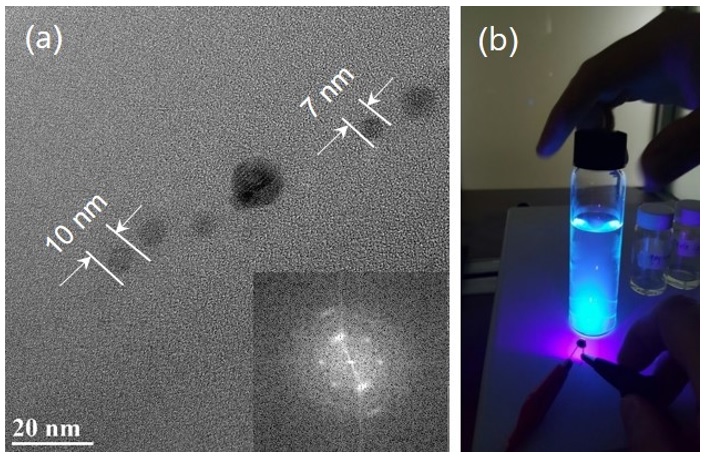
(a) HRTEM image of GQDs. (b) Blue emission of synthesized GQD dispersion under UV light irradiation.
Figure 3(a) shows the UV–Vis transmittance of all-graphene-based thin films composed of spray-coated rGO thin films and GQDs on top of the transferred CVD-graphene bottom electrode. The constructed device exhibited good transparency and flexibility, as evidenced by the inset in Figure 3(a). Two sensor devices, each with two silver electrode contacts and an effective area of 1 cm by 1 cm, are represented by two rectangles with dotted lines. The transmittance of the fabrication device can be visually assessed through the "wave" character and the visual details hidden under the device. The Raman characteristics of the all-graphene platform are displayed in Figure 3(b). In the figure, there are two significant peaks, D and G. A strong 2D peak suggests an out-of-plane vibration mode due to lattice disorganization, and a combination of the D and G peaks gives a D+G peak near 2906 cm. Despite the fact that the analyzed sample contains three forms of graphene nanostructures, graphene, rGO, and GQDs, the observed signal is dominated by rGO sheets. This means that rGO sheets are important and have a large impact on the optical characteristics of an all-graphene platform. All Raman characteristics of graphene-based materials were observed, according to our findings.

(a) UV–Vis transmittance, (b) Raman spectra, and (c) measured resistance change under the bending test of the fabricated all-graphene-based UVPD device.
The effective area (1×1 cm) of the all-graphene-based device fabricated on a PET substrate, which was electrically contacted, could be bent with different bending radii. The variation in the device’s resistance as a function of bending radius was measured and is plotted in Figure 3(c). The results indicated that the electrical performance of all graphene-based device platforms is stable under mechanical transformation.
SEM and AFM measurements were carried out to characterize the surface morphology of the all-graphene-based film, as shown in Figure 4(a) and Figure 4(b), respectively. rGO sheets randomly stack and overlap one another, as shown in Figure 4(a), and the produced GQDs are randomly spread across the surface of the rGO sheets. There were also long and broad wrinkles/folds on the surface. As a result, the films exhibited a large number of structural flaws. This is characteristic of films made by spray-coating using a solution approach. In fact, when spray-coating rGO and GQD dispersions onto a warmed PET substrate, the rGO sheets abruptly freeze when they toughen the hot substrate, causing the solvent to flash evaporate and roughen the surface. Similarly, two-dimensional rGO sheets with wrinkles/folds were clearly observed in the AFM image, as shown in Figure 4(b).

(a) SEM and (b) AFM images measured from the all-graphene-based film.
Figure 5shows the current-voltage graph linked to the operability of the constructed device that was measured. The active layers of the rGO/GQDs and the interdigitated-bottom graphene electrode display ohmic contact behavior with a linear I-V curve and no rectifying characteristic. This result implies that the generated graphene multidimensional structures linked together and formed a homogenous structure favorable for electron transfer. The two-dimensional reduced graphene oxide layer, in particular, plays a key role in building a network for the transfer of photogenerated carriers as well as a linked layer between graphene quantum dots and bottom electrodes. The dark current is approximately 6.03 µA at a bias of 2 V, while its value increases to 10 µA when the device is illuminated (l = 380 nm, 0.5 mW/cm). The variation in the current is a good demonstration of the optical sensing operation of the fabrication device. The explanation for the increase in current when the device is illuminated is due to photon absorption in the GQDs and rGO active layer, which gives rise to electron transfer from to * in sp aromatic domains and from to * in C = N and C = O bonds8.

I-V characteristic measurement with and without UV illumination (0.5 mW/cm2).

(a) Photogenerated current and (b) photoresponsivity of the all-graphene platform at 2 V bias under illumination with different wavelengths.
According to Figure 6(a), by periodically turning the UV light on and off, the platform of this device may be reversibly switched between low and high conduction states with good stability and reproducibility. The rise and decay times for this structure are predicted to be 100 s for both the rising and falling edges, which is slower than other graphene-based photoconductors built on a hard substrate. The low-temperature solution method is to blame for this unexpected performance. Defective surfaces, such as wrinkles/folds, trap photogenerated electrons, resulting in longer rise and decay durations, as inferred from TEM images. Another explanation is that functionally related groups remained on the rGO surface due to an incomplete reduction process. These functional groups take part in the surface reaction with oxygen molecules in the surrounding environment. A delay in response time is also caused by this surface reaction. Under a bias of 2 V, the responsivity of the transparent and flexible all-graphene-based UVPD device at different wavelengths is shown in Figure 6(b). The device is sensitive to ultraviolet light with a wavelength range of 200 nm to 400 nm and a peak responsivity between 280 and 390 nm. A visible-blind feature is also included in the device.
Discussion
As a zero-dimensional graphene material, GQDs also have the properties of graphene, including unique quantum confinement and edge effects. GQDs have a persistent fluorescence and a variable bandgap due to these features. GQDs can be used as an active layer in ultraviolet sensor devices because of their great properties. The following is the operating mechanism of the GQD/rGO active layer for UV sensing in more detail: The absorption photon energy of incident light (380 nm) stimulated the carriers transferred in GQDs from E to E. According to Zhang et al., there is a high possibility that the excited carriers will be separated at the rGO and GQD junction. When an external electric field is applied to the device, the produced electrons and holes will travel in opposite directions to the underlying graphene conductive substrate, resulting in an increase in electrical current9, 10, 11. As a result, utilizing this architecture significantly suppresses electron-hole pair recombination and facilitates charge carriers to graphene electrodes. Consequently, a photocurrent (I) is generated when the device is illuminated under UV light. Thus, the value of the photocurrent under UV illumination is often used to assess UV sensing performance.
In addition, because of the low-temperature solution process utilized, this structure is very straightforward to produce, making it ideal for flexible substrates. This is a promising option for noninvasive human fitness and health monitoring devices that do not modify the person’s vital signs, such as wearable health trackers.
The responsivity of our all-graphene-based photodetector was calculated with the following formula12, 13, 11, 14:
where R is the responsivity, I and I are the illuminated current (l = 380 nm) and dark current, respectively, P is the power density of incident light, and S is the effective area of the rGO/GQDs active layer. Our results indicate that the responsivity of the fabricated device was 7.94 mA/W, which is comparable to that of other nanomaterial-based photodetectors. However, it is significantly higher than that of other flexible and transparent photodetectors.
Comparison of the performance of photodetectors on different (rigid or flexible) substrates
|
Active materials |
Substrate |
Excited wavelength (nm) |
Photo-responsivity (A/W) |
References |
|
ZnO NRs |
Glass |
400 |
1.11 x 10⁻³ |
|
|
Ag NPs/ZnO NRs |
Glass |
400 |
6.52 x 10⁻³ |
|
|
ZnO nanorods arrays/GQDs |
GaN |
365 |
34 x 10-3 |
|
|
WS2 |
Polyimide |
450 |
0.83 × 10⁻⁶ |
|
|
Graphene/CH3NH3PbI3 |
Polyimide |
520 |
3 x 10⁻⁶ |
|
|
Graphene/Cu2O/Cu |
PET |
550 |
86 x 10-3 |
|
|
WS2-graphene |
flexible ITO |
White light |
36 x 10-3 |
|
|
Graphene/rGO/GQDs |
PET |
380 |
7.94 x 10⁻³ |
This work |
Conclusions
Using a solution synthesis process of rGO and GQD coatings on interdigitated graphene bottom electrodes transferred to a PET substrate, we introduce a new, fully carbon-based structural platform exclusive for the fabrication of optoelectronic devices on a flexible and transparent substrate. The method is low-cost and scalable. Research results have shown that this new structure is capable of detecting ultraviolet rays. We argue that this platform opens another approach for the cost-effective production of transparent and flexible photodetector applications.
Author contribution
Hoang Hung Nguyen and Huynh Tran My Hoa contributed equally to this work. T.V.C. conceived and directed the research. H.H.N. carried out measurement system setup and helped in all measurements. H.T.M.H. performed the nanomaterials synthesis and fabricated the photodetector device. H.P.P. helped with the graphene growth on copper foil. V.Q.D. contributed measurement and helped with the analysis. T.V.C. and H.T.M.H. analyzed the results and wrote the paper. All authors discussed the results and commented on the manuscript, and approve the final manuscript.
Conflicts of Interest
The authors declare no conflict of interest.
Acknowledgments
This research was supported by Vietnam National Foundation for Science and Technology Development (NAFOSTED) under grant number 103.02-2018.352.
Abbreviations
UVPD: ultraviolet photodetectors
GO: graphene oxide
rGO: reduced graphene oxide
GQDs: graphene quantum dots
PET: polyethylene terephthalate
DFT: density functional theory
HRTEM: high-resolution transmission electron microscopy
SEM: scanning electron microscope
AFM: atomic force microscope