

Variable Pulse Density Modulation for a Buck-Type Three-Switch Current Source Rectifier
- Ho Chi Minh City University of Technology, Vietnam National University Ho Chi Minh City (HCMUT), Ho Chi Minh City, Viet Nam
Abstract
With flexible voltage adjustment without an intermediate DC/DC converter, short-circuit protection, self-starting, high reliability, and three-phase current source rectifiers (CSRs) are being widely used in high-power medium-voltage applications and low-power low-voltage applications. Modulation methods significantly affect the performance of CSRs and can be categorized into offline modulation methods, such as selective harmonic elimination/compensation pulse width modulation (SHE/SHC-PWM), and online modulation methods, such as space vector pulse width modulation (SV-PWM) and carrier-based pulse width modulation (CB-PWM). The SHE/SHC-PWM is popular in high-power medium-voltage applications that do not require a fast dynamic response and have a low switching frequency. Online modulations considerably improve the dynamic response and performance of the CSR; however, high computational power, such as digital signal processors (DSPs), is required at higher switching frequencies, leading to greater system complexity and cost. In this paper, an offline method based on variable pulse density modulation (VPDM) of power switches to synthesize sinusoidal input currents and control power transfer with pulse width modulation (PWM) is proposed. The proposed modulation is applicable to the three-switch buck-type VIENNA rectifier, showing the capability of improving the input current total harmonic distortion (THD) with respect to the SHE-PWM and is comparable to online modulations at a sufficiently high switching frequency. The simulation and experimental results basically prove the feasibility of the proposed modulation.
INTRODUCTION
Traditional three-phase AC/DC converters, namely, diode rectifiers and thyristor-based rectifiers, have been widely used as the first stage in many power electronic configurations to provide unidirectional or bidirectional DC power in an uncontrolled or phase-controlled manner. With these configurations, the input power quality will be low; specifically, the input current total harmonic distortion (THD) will be high, the input power factor will be low, there will be high ripples on the DC output, low efficiency, and bulky AC and DC filters. On the other hand, power quality regulations on the user side are increasingly gaining attention with recent updates on related standards 1, 2. Transistor-based rectifiers have therefore been developed to overcome these weaknesses and are divided into two groups, voltage source rectifiers (VSRs) and current source rectifiers (SRs), according to the energy storage component on the DC side. VSRs have been thoroughly studied and greatly improved for widespread industrial application because of their suitability for many nonlinear controllers3, 4, simple structure, and low losses. However, in some voltage step-down applications requiring a wider input voltage range and limited output current in cases of output short circuiting, the CSR configuration (see Figure 1) is preferred to adding another DC/DC stage after the VSR.

Three-phase six-switch current source rectifier
Moreover, CSRs are widely used not only in medium-voltage high-power applications (with symmetric gate commutated thyristors or gate turn-off thyristors) due to their simple structure and short-circuit protection5 but also in low-power systems such as motor speed control6, induction heating7, electric vehicle chargers 8, and telecommunication power supplies9. The modulation methods used in CSRs can be divided into two groups: offline and online. Among offline methods, selective harmonics elimination/selective harmonics compensation (SHE/SHC) pulse width modulation (PWM)10, 11, 12, 13 is often used for medium-voltage high-power applications; this method does not require a fast dynamic response and has a low switching frequency to reduce switching losses. The sinusoidal PWM14, 15, space vector PWM16, 17, 18, and carrier-based PWM 19, 20 are online methods. A typical CSR is a six-switch rectifier, as illustrated in Figure 1, in which unidirectional switches can be implemented with reverse blocking IGBTs (RB-IGBTs) or diodes in series with MOSFETs or IGBTs. Online modulations could significantly improve the dynamic response and performance of CSRs but require much greater computational power from digital controllers (microcontrollers or digital signal processors). With the growth of fast switching devices, such as SiC and GaN transistors, the computational power required for implementing faster switching frequencies (150 kHz and above) and complicated control algorithms will impose serious challenges on digital controllers or even field programmable gate arrays (FPGAs), leading to significant obstacles in designing converters with online algorithms21.

Three-phase three switch current source rectifier and sector designation
The number of active switches in the six-switch rectifier can be reduced with the three-switch rectifier (illustrated in Figure 2a), as proposed for the first time in 22; applying an offline PWM method on GTOs in23; and space vector PWM (SV-PWM) with a switching frequency below 35 kHz in 24, 25, 26, 27, 28, 29, 30, 31, reaching an efficiency of 95.1%, as reported in 26; and an input current THD of 6.9% for an open loop SV-PWM 25. Carrier-based PWM can also be used for this topology with a switching frequency below 10 kHz, achieving an input current THD below 5% in simulations32, 33, and at 7.3% in experiments 34. Similar simulated input current THD results have also been reported for sine PWM at 30 kHz 14, 20 kHz35 and 10 kHz15.
One of the main objectives of the above studies was to improve modulation methods to achieve an input current THD below 5% for all three phases, as standardized in12; however, the switching frequency is normally less than 35 kHz due to efficiency degradation at higher frequencies 18. An offline variable pulse density modulator (VPDM) specifically designed for high switching frequency, aimed at a unity power factor and low input current THD, has been proposed for the three-switch current source rectifier (3SWCSR) and will be presented in this paper. The simulation results confirmed the feasibility of the proposed modulation algorithm with an input current THD of 8.6% at a 38.4 kHz switching frequency and 4.3% at 174 kHz. The experimental results at a 38.4 kHz switching frequency also confirmed the proposed solution. Next, a comparison between the VPDM and space vector PWM (SVPWM) is presented, followed by simulation and experimental results.

Current flow and ON switch status
VARIABLE PULSE DENSITY MODULATION FOR ACTIVE RECTIFIERS
Assuming a balanced three-phase power supply, with the instantaneous phase voltages described in (1) (in which U [V] is the phase voltage magnitude and ω [rad/s] is the angular frequency), is connected to the 3SWCSR, the input voltage sectors can be designated as shown in Figure 2b. The following analysis will be performed for sector 1 (v > 0 > v > v) and can be performed in a similar manner for other sectors.
On- (k = a, b, c) (S = 0 means the corresponding switch is turned off, S = 1 indicates that the corresponding switch is in an on-state) for a switching state j = (SSS) in the online SV-PWM, and the proposed VPDM will be implemented on the basis of the following assumptions 29 for simplicity:
-
The voltages on the input filter capacitors (Cf,ab, Cf,bc, Cf,ca) of the 3SWCSR are sinusoidal and in phase with the main phase voltages. Hence, the voltage drops on the filter inductors (Lf,a, Lf,b, and Lf,c) can be neglected.
-
The main currents (ia, ib, ic) are assumed to be equal to the fundamental component of the rectifier input currents (irec(1),a, irec(1),b, irec(1),c); therefore, the reactive currents due to the filter capacitors are also neglected.
-
With a sufficiently large DC output inductor, the current through the output inductor IDC is assumed to be constant, meaning that the high-frequency ripple due to the switching operation is neglected.
-
With the above assumptions, the SV-PWM for 3SWCSR will be described next for comparison with the proposed VPDM later on the same topology.

3SWCSR conduction states in sector 1 (van > 0 > vbn > vcn)

Current space vector
Current Space Vectors
|
Vector |
Switches |
Input currents |
|
Vdc | ||||
|
Sa |
Sb |
Sc |
irec,a |
irec,b |
irec,c | |||
|
|
1 |
0 |
1 |
IDC |
0 |
- IDC |
|
van - vcn |
|
1 |
1 |
1 | ||||||
|
|
0 |
1 |
1 |
0 |
IDC |
- IDC |
|
vbn - vcn |
|
1 |
1 |
1 | ||||||
|
|
1 |
1 |
0 |
- IDC |
IDC |
0 |
|
vbn - van |
|
1 |
1 |
1 | ||||||
|
|
1 |
0 |
1 |
- IDC |
0 |
IDC |
|
vcn - van |
|
1 |
1 |
1 | ||||||
|
|
0 |
1 |
1 |
0 |
- IDC |
IDC |
|
vcn - vbn |
|
1 |
1 |
1 | ||||||
|
|
1 |
1 |
0 |
IDC |
- IDC |
0 |
|
van - vbn |
|
1 |
1 |
1 | ||||||
|
1 |
0 |
0 |
0 |
0 |
0 |
0 |
0 | |
|
0 |
1 |
0 | ||||||
|
0 |
0 |
1 | ||||||
|
0 |
0 |
0 | ||||||
A. Online Space Vector Pulse Width Modulation of Input Currents
For the 3SWCSR in Figure 2a, S in the on-state (S = 1) connects node k to one branch of the rectifier via a block diode D (or D) corresponding to the positive (or negative) current from the mains to the rectifier. It is possible to identify current paths for all switching states. Depending on whether the current direction between the mains and the rectifier is positive (i = I) or negative (i = -I), a mains phase (a, b, c) will be connected to node X (or node Y), as in Figure 3, for the same switching state; alternatively, no output nodes (indicated by node O) will be connected to the mains phase. For example, if state j = (101), as illustrated in Figure 4a, S and S are turned on, allowing currents i = I (a connected to X) and i = -I (c connected to Y) to flow between phase A and phase C, forming a current space vector [XOY]. All possible switching states are shown in Figure 4 for sector 1. All the switching states and corresponding current space vectors are shown in
Online SV-PWM at switching frequencies below 35 kHz was fully developed with high performance in24, 25, 26, 27, 28, 29, 30, 31, 32, 33, 34, in which a particular switching state sequence was proposed to reduce the input current THD due to glitching at sector boundaries in29. In this modulation, each sequence includes two active states and one free-wheeling state, which are symmetrically arranged. For example, in sector 1, the symmetric sequence (101)-(110)-(010)-(110)-(101) is applied, where j = (SSS) indicates a combination of the three switches, state ‘1’ means the corresponding switch is turned on, and state ‘0’ indicates that the corresponding switch is in an off-state. The relative on-times for switches in active and free-wheeling states are determined as in (2) - (5) [29], in which is the modulation index, I is the magnitude of the input phase currents, I is the DC current, and v, v, and v are instantaneous input phase voltages 25.

VPDM method in sector 1
From equations (2) - (5), to implement the SV-PWM, the controller must continuously sample the instantaneous input phase voltages before each switching cycle and calculate all the relative on-time voltages using trigonometric expressions. For higher switching frequencies, the available time for calculations will be shorter, and some predictive algorithms might be needed or the switching frequency could not increase much. This problem can be solved with offline modulations, such as pulse density modulation (PDM), in which relative on-times can be predetermined and saved in lookup tables. PDM was first applied to VSR in 199237, in which an active-voltage clamped resonant DC link (ACRDCL) was used to divide voltage vectors in each sampling period into four blocks to reduce errors introduced by selecting the closest vector in the SV-PWM. However, calculations on the d-q reference frame still need to be performed on the DSP; at the same time, a predictive algorithm is needed for current estimation on the ACRDCL due to calculating limitations of the DSP. In 38, a PDM algorithm was proposed for a three-phase to single-phase matrix converter in induction heating applications with zero-voltage switching (ZVS) on bidirectional switches owing to the high-frequency AC load current to synthesize sinusoidal input currents at a unity power factor. In addition to those two studies, there have been no publications on the application of the PDM to current source rectifiers. The fundamentals of PDM control will be described next.
B. Variable Pulse Density Modulation (VPDM)
In this section, a VPDM algorithm is proposed for a hard-switching 3SWCSR at frequencies less than 50 kHz to simplify the implementation and analysis, as illustrated in Figure 6 for input sector 1. Each sector is divided into four equal blocks, and each block includes sixteen switching cycles. For an exact 50 Hz main cycle, a perfect fit should require 768 switching cycles, leading to a 38.4 kHz switching frequency and no line synchronization. An offline pulse distribution pattern can be used to synthesize three-phase input currents, while power transfer can be regulated by pulse width modulation.
Switching states and current equations
|
Interval/Sector |
Switching States |
Current equation |
Source | ||
|
X |
Y | ||||
|
I |
1 |
SAX |
SBY/SCY |
IA = IB + IC |
vab, vac |
|
2 |
SAX/SBX |
SCY |
IC = IA + IB |
vbc, vac | |
|
II |
3 |
SBX/SAX |
SCY |
IC = IA + IB |
vbc, vac |
|
4 |
SBX |
SAY/SCY |
IB = IA + IC |
vbc, vba | |
|
III |
5 |
SBX |
SCY/SAY |
IB = IA + IC |
vbc, vba |
|
6 |
SBX/SCX |
SAY |
IA = IB + IC |
vba, vca | |
|
IV |
7 |
SCX/SBX |
SAY |
IA = IB + IC |
vba, vca |
|
8 |
SCX |
SBY/SAY |
IC = IA + IB |
vca, vcb | |
|
V |
9 |
SCX |
SAY/SBY |
IC = IA + IB |
vca, vcb |
|
10 |
SCX/SAX |
SBY |
IB = IA + IC |
vcb, vab | |
|
VI |
11 |
SAX/SCX |
SBY |
IB = IA + IC |
vcb, vab |
|
12 |
SAX |
SCY/SBY |
IA = IB + IC |
vab, vac | |
Considering a balanced three-wire three-phase system, the distribution pattern must ensure that the algebraic sum of the instantaneous input currents is zero at all times, meaning that the current will exit one input phase to spread into the other two phases or that two input phase currents will flow into the remaining phase. For example, considering sector 1 (v > 0 > v > v), the current going out of phase A should be equal to the sum of the currents going into phase B and phase C (I = I + I), and power is being transferred from V and V sources to the load, with S or S being used to connect node b or node c to node Y, while S is used to connect node a to node X. In the next sector, sector 2, a similar condition exists with two available positive voltage sources of V and V, in which S or S is used to connect node a or node b to node X, while S is used to connect node c to node Y. Instantaneous current going into phase C equals the sum of the currents going out of phase A and phase B (I = I + I).
In each sector, the magnitude of the maximum instantaneous current in (6) should be proportional to the magnitude of the highest absolute instantaneous line-to-line voltage, with the expression of this instantaneous line-to-line voltage as (7) for sector 1.
The highest absolute instantaneous line-to-line voltage is created from two (out of three) input phase voltages and provides power to the two-wire load via the DC link voltage. Due to the symmetry of the three-phase input system, the role of the input phases can be swapped in the input sectors to form the six-pulse rectified voltage, as shown in Figure 2b. If there are enough blocks in each sector, it can be assumed that in one block, the instantaneous line-to-line voltage is practically constant 38. Let be the pulse density of the switches used to create the line-to-line voltage in that block; then, the average line-to-line voltage in the block (VPDM) will be proportional to this pulse density, as in (8):
From (6-8), we can see that the VPDM is proportional to , as in (9):

Noninterlacing PDM pattern
On the other hand, for sinusoidal input phase currents, the total three-phase power transferred from the source to the load should be constant; therefore, the pulse density functions must be regulated so that the average line-to-line voltage VPDM is constant. Because the transferred power is proportional to the square of the available voltage for a given pulse density, the output power can be maintained constant if the pulse density is implemented as in (10)38:
The function is quantized (for a digital implementation of the algorithm), plotted for the number of blocks of the implemented algorithm in Figure 6b, and applied for the phase with the highest absolute instantaneous voltage; for example, in sector 1, it is phase A, and the density of the other two input phases can be determined by (6) and (11).
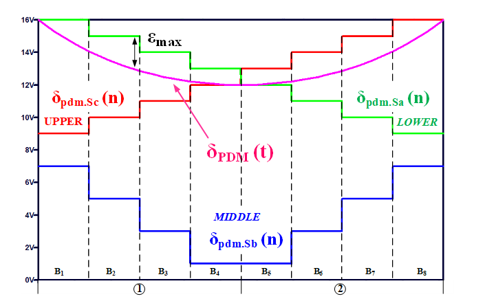
In Figure 6b, the exact time function of pulse density δ(t) for the VPDM algorithm is depicted, together with quantized pulse density functions for the input phases (UPPER), (LOWER) and (MIDDLE). To implement the VPDM algorithm, PDM patterns for the most positive phase (UPPER) and the most negative phase (LOWER) are taken from a preset lookup table (for example, in the FPGA), and the last PDM for the third phase should be determined from a logical combination of the first two PDM patterns to fulfill the requirement of I + I + I = 0 in a three-wire three-phase system.

Hybrid and interlacing PDM pattern

Current stress in semiconductor devices of 3SWCSR
For line frequency synchronization, the number of PDM blocks and the switching frequency should satisfy (12), in which is the switching frequency [Hz]; is the line frequency [Hz]; is the PDM block length (number of switching cycles per PDM block) [pulse/block]; and is the number of blocks per sector [block/sector]. The PDM block length should be large to ensure good magnitude resolution (16, 32, or 48 or more). However, this approach would reduce the temporal resolution. Furthermore, a large number of PDM blocks Bb (corresponding to a small PDM block length) are required to ensure effective line frequency synchronization, and the details of the proposed solution for VPDM are described in section IV of this paper.
A simple PDM pattern is drawn in Figure 7, which is applied to the reference current vector, as illustrated in Figure 6a, in which the Sa, Sb, and S switches have pulse densities of 15/16, 5/16, and 10/16, respectively. Due to quantization error, it can be predicted that at several positions in each sector (e in Figure 6b), there could be some current glitches. For a given pulse density, the distribution pattern in a block can also affect the input waveform, similar to the switching sequence of active and zero vectors in SV-PWM. Two other PDM patterns can also be used for 16-pulse blocks, as shown in Figure 8, where the hybrid pattern drawn in Figure 8a is a combination of the noninterlacing pattern shown in Figure 7 and the interlacing pattern depicted in Figure 8b. The noninterlacing PDM pattern provides the best overall efficiency among the three VPDM strategies with the same PDM varying algorithm, while the interlacing pattern gives a better power factor. Next, the simulation results of SV-PWM and VPDM on the 3SWCSR will be presented, and a performance comparison and evaluation will be performed.
SIMULATION RESULTS AND DISCUSSION
To verify the feasibility and evaluate the AC input and DC output quality of a 3SWCSR model with the proposed VPDM algorithm, a 5 kW, 38.4 kHz rectifier, with the design specifications given in
A. Semiconductor Voltage and Current Stresses
In this section, the stresses on semiconductor components are calculated according to the operating parameters of the converter, which is important in system design and provides a basis for selecting suitable components to verify the feasibility of the algorithm via simulation and experimentation. The voltage stress can be quickly determined from the magnitude line-to-line voltage of the three-phase system under the maximum allowable voltage deviation (10% in Vietnam), as in (13). However, a voltage headroom of 50% should be used as the absolute voltage on the component to account for transient glitches and harmonic voltages.
Current stresses are harder to determine because they are related to the modulation algorithm being used, the switching frequency, and other conditions in the source and load. RMS values are necessary to determine the current rating and power losses of the component in the design procedure. In VPDM, the current waveform depends on the number of blocks per sector, the block length, the PDM pattern, and the pulse width. All these parameters are selected to implement the pulse density curve (10) as closely as possible in each sector, and the analysis of the current waveform is not considered in this paper. However, it can be assumed that with a large enough number of blocks, sinusoidal input currents can be implemented, and the power transferred to the load is the same for both the SV-PWM and VPDM. Therefore, the current stresses are determined by calculations deduced for the SV-PWM as a reference, and the discrepancy in the simulated current stresses for both algorithms is evaluated.
The RMS value of the input current is now considered to determine the current stresses on diodes and switches. Due to the symmetry of the three-phase system, it is sufficient to study only one input phase. For example, the local RMS value of the phase A input current over a switching cycle can be determined from the instantaneous i current (14), giving the square RMS value over a switching cycle T in (15). The global square RMS value (over a mains cycle T) of the phase A input current is then given in (16).
Simulation Parameters
|
Parameter |
Value | ||
|
Power Supply |
3 phases, 220 V/380 V – 50 Hz | ||
|
Rated Power Pn |
5 kW | ||
|
PF |
> 0.9 | ||
|
THDi |
< 5% | ||
|
AC Filter |
Cf |
1.5 µF | |
|
Lf |
5 mH | ||
|
Rdump |
45 Ω | ||
|
DC Filter |
Cdc |
1000 µF | |
|
Ldc |
2 mH | ||
|
VPDM |
BB |
8 Block | |
|
nB |
16 pulse | ||
|
fs |
38.4 kHz | ||
Comparison Of RMS Current Stresses In Simulations AndCalculations
|
Current |
Analytics [A] |
SIMULATION SV-PWM (M = 0.85) |
SIMULATION PDM (D = 0.95) | ||
|
Value [A] |
Deviation [%] |
Value [A] |
Deviation [%] | ||
|
|
9.3068 |
9.3946 |
0.9 |
9.7365 |
4.6 |
|
|
6.5809 |
6.6545 |
1.1 |
6.8986 |
4.8 |
|
|
5.318 |
4.9385 |
7.7 |
4.5015 |
15.4 |
|
|
12.5 |
12.578 |
12.544 | ||

Simulation and control scheme

Simulation results
By examining the current waveforms on the phase A leg, the RMS values of the currents in the corresponding switch S and diodes can be estimated by (17) - (19) and are given in Figure 9. The analytical and simulated current stresses on these components for both the SV-PWM and VPDM simulations are compared in
B. Simulation Results and Discussions
To evaluate the performance of the proposed VPDM algorithm for the 3SWCSR scenario, a simulation model with a 5 kW rating was built, as shown in Figure 10, in which the load is a resistor in parallel with the output capacitor C and the CSR is acting as a variable DC voltage source. The control scheme is shown in Figure 10b, where a 38.4 kHz PWM signal is created by comparing the demand DC voltage and the real DC voltage. PWM pulses are distributed to SSS according to the preset VPDM pulse mapping for the corresponding input sector and are detected by a zero-crossing detector (ZCD). Both SV-PWM (at a 12 kHz switching frequency) and VPDM (at a 38.4 kHz switching frequency) will be simulated.
In Figure 11, the input current i, phase A input voltage V, and DC output voltage VDC waveforms are presented for both the SV-PWM and VPDM algorithms. Both algorithms create a high power factor of 0.99 and a low ripple DC output voltage at the rated power. The SV-PWM can provide a high-quality input current with a THDi of 3.3%, while the VPDM produces a higher harmonic content with a THDi of 8.6% (the THD is calculated for harmonics up to the 30th). An FFT analysis was performed on the input current waveform created by the VPDM, revealing the good filtering effect of the input filter; however, high magnitudes (over 5%) occurred at the 23rd and 25th harmonics, leading to high THDi. The higher order structure of the CSR with respect to VSR could be the reason, due to the possibility of resonances among the input filter and output filter components, leading to some high harmonics. Furthermore, the selection and distribution of PWM pulses in VPDM should affect the current THD but will not be considered in this paper. The relative power losses of VPDM (93.28% efficiency) and SVPWM (95.62% efficiency) were analyzed, and the power losses on the filters were significantly different, as shown in Figure 12b. The power losses on filters (and other supporting components) in the VPDM are five times greater than those in the SVPWM due to the addition of the R and ESRs of inductors and capacitors needed to achieve low harmonic distortion in the VPDM. This can be improved by using different PDM patterns or higher switching frequencies.
To demonstrate the effect of the switching frequency in VPDM, a simulation with a 174 kHz switching frequency, Bb = 36, and n = 16 was performed with the resulting waveforms shown in Figure 13.

FFT analysis and power loss comparison (in simulation)

VPDM 174 kHz (THDi 4.3%; PF 0.9962)
In Figure 13, the simulated input current THD is reduced from 8.6% at a 38.4 kHz switching frequency to 4.3% at 174 kHz. The error ε would not considerably affect the input current waveform because at a higher switching frequency, the VPDM should have a higher resolution to closely approximate the pulse density given in (9). On the other hand, current glitches at sector boundaries are still significant, as shown in Figure 12, similar to online algorithms such as the SV-PWM in 24, 25, 26, 27, 28, 29, 30, 31.

VPDM Synchronization method
Next, line frequency synchronization and PDM patterns are discussed, followed by a description of the experiments on a prototype using MOSFET with a 38.4 kHz switching frequency.
SYNCHRONIZATION METHOD FOR THE VPDM
In practice, a small variation in line frequency is allowed in all standards; hence, line frequency synchronization must be performed. For online algorithms, such as SV-PWM, this could be a challenge in power converters when the switching frequency passes 100 kHz. For the proposed offline VPDM, sampling is unnecessary; however, the line period is not necessarily an integer multiple of the PDM block, necessitating a line frequency synchronization algorithm for experiments.
Due to the symmetry in pulse density between two adjacent sectors, only one lookup table (LUT-1) is needed to store the pulse density value for each block. In FPGA, a counter Bb is used to maintain the block index for retrieving the pulse density value of the current block. After obtaining this pulse density, the corresponding PDM pattern can be determined with another lookup table (LUT-2f), in which another counter n is used to track the current switching cycle in the block. Let B be the maximum possible number of blocks, be the allowable frequency variation, and Bbs be the block index at which line frequency synchronization starts for that sector. The nominal line frequency and the switching frequency will set BB (an integer value), while B should be an integer and chosen according to (20).
A flowchart of the proposed line frequency synchronization algorithm for an FPGA is shown in Figure 14. At the transition between an even sector and an odd sector, for example, from sector 12 to sector 1, the counter B starts at the lowest index and increases until it reaches the highest index BB in the LUT-1. When the counter value is equal to B, the FPGA should start the line frequency synchronization algorithm to account for the highest allowable line frequency. If the line frequency is low enough, the counter should be able to reach the highest index B and stay there until the sector transition. After the sector transition, when the odd sector starts, the counter will decrease to the lowest value index in the LUT-1 and stay there until the next sector transition. This process is repeated at the transition between an even sector and an odd sector; hence, six times the input current waveform is synchronized with the input voltage waveform in any main period.
With the proposed line frequency synchronization method, for any main period shorter than the total time of all blocks in LUT-1, the FPGA can easily detect sector transitions before reaching the highest index in LUT-1. For example, if the line frequency is 5% higher than the nominal frequency, which means that it is 52.5 Hz, then the transition should be approximately 7.6 blocks (for a 38.4 kHz switching frequency, and B is 8). On the other hand, if the line frequency is lower than the nominal value, the FPGA should reach the end of LUT-1 and wait for the sector transition. A large pulse density is maintained for the most active input phase so that at the peak of the current waveform, distortion can be limited, leading to low input current harmonic distortion. The experimental results in the next section prove the feasibility of the proposed modulation method and the proposed line frequency synchronization algorithm for 3SWCSR.
V. EXPERIMENTAL RESULTS AND DISCUSSION
The simulation results in section III prove the feasibility of the offline VPDM, combined with the line frequency synchronization method proposed in section IV, applied to the 3SWCSR. To verify the practical performance of the converter, a 2 kW – 38.4 kHz prototype of the 3SWCSR, as shown in Figure 15a, with the basic parameters in

Experimental prototype
In Figure 16, the phase A input current i waveform (red), phase A input voltage v waveform (blue), gating signals for S (D), S (D), and S (D), gating signal for S in the positive mains half-cycle (D), and negative mains half-cycle (D) are shown. Input voltage (red) and input current (blue) waveforms for phase A are shown in Figure 17a, and the output DC voltage V, input currents i and i waveform, and input voltage v waveform are shown in Figure 17b. Waveforms were obtained by RIGOL DS-1102D (2 channels) and Gwinstek GDS-2064 (4 channels) DSOs. Harmonic distortion and the power factor were measured by a HIOKI CM3286-01 AC clamp power meter.
From the experimental results, the feasibility of the VPDM on the 3SWCSR has been shown for a low ripple (6.25%) DC output voltage, with a good input power factor (better than 0.9) and better input current THD (15.11%) than that of a diode rectifier (normally higher than 30%), or that of a basic SV-PWM algorithm (16.6%) 25. The 3SWCSR has been tested at a 38.4 kHz switching frequency suitable for power switches under hard switching, with current glitches at sector boundaries leading to an input current THD higher than the limit suggested by the IEEE-519 standard1, which is in good agreement with the simulation result of 8.6% presented in section III. The experimental results show a high power factor close to the results obtained in the simulation, proving that the synchronization process is well implemented to ensure phase synchronization between the current signal and the source voltage. However, the input current harmonics are more different in the experiment because the effects due to resonance between filters and parasitic components are ignored in the simulation. However, with these experimental results, the feasibility of the proposed algorithms has been proven, and it is possible to increase the switching frequency to achieve better input quality, depending on the power switches being used.
CONCLUSION
This paper proposed an offline variable pulse density modulation (VPDM) algorithm for a three-switch current source rectifier (3SWCSR) to achieve a high input power factor and reduced input current total harmonic distortion, with simple and effective implementation, especially when increasing the switching frequency. The algorithm can control the output voltage of the 3SWCSR over a wide range and needs to be implemented only by a PI controller, while the three-phase input sinusoidal waveform is achieved by means of offline FPGA-based lookup tables without any sampling operation Therefore, it is advantageous to increase the switching frequency of the system. In addition, a synchronization algorithm with respect to the grid frequency is proposed to ensure the operation of the converter under changing grid conditions. The simulation and experimental results basically prove the feasibility of the proposed modulation, with a low-output DC voltage ripple of 6.25%, a high input power factor of 0.94, and an input current total harmonic distortion that is half of that in traditional uncontrolled rectifiers. In addition, simulation results also show that when the frequency is increased to 174 kHz, the input current harmonic quality is comparable to that of online algorithms.

Gate driver signals in FPGA and input waveforms.

Experimental waveform results
Acknowledgments
We acknowledge Ho Chi Minh City University of Technology (HCMUT) and VNU-HCM for supporting this study.
list of abbreviations
CSRs: current source rectifiers
SHE/SHC-PWM: selective harmonic elimination/compensation pulse width modulation.
SV-PWM: space vector pulse width modulation
CB-PWM: carrieer-based pulse width modulation
DSP: digital signal processor
VPDM: Variable pulse density modulation
LUT: Look-up table
ZCD: Zero-crossing detector
ACRDCL: Active-voltage clamped resonant DC link
authors’ constribution
Thuong Ngo-Phi proposed the research idea and conducted simulations and experiments.
Nguyen Dinh Tuyen contributed to the technical background and proof reading.
Nam Nguyen-Quang contributed to the technical background, hardware implementation, and proof reading.
funding
We acknowledge Ho Chi Minh City University of Technology (HCMUT), VNU-HCM for partial funding this study.
conflict of interest
The authors confirm that they do not have any conflict of interest in completing this paper.